How to Get Your KiCad PCB Design Ready for Automated Assembly – KiCad 6 Tutorial
Tutorial on generating assembly files for automated PCB assembly (PCBA) from KiCad 6 open-source schematic and PCB designing software.

This is a follow-up post to our previous tutorial – How to Get Your KiCad PCB Design Ready for Fabrication. For those who don’t know, KiCad is a free and open-source Electronic Design Automation (EDA) suite originally developed by Jean-Pierre Charras and is now being actively maintained by a group of developers. It has everything needed to create complex multi-layer PCBs as you wish. It has limitless customization options, thanks to the open-source design and scripting tools. KiCad 6 has been released recently. KiCad 6 is going to make the platform appealing to an even wider group of people including students and professionals. KiCad v5 had so many ambiguous aspects that many beginners found it a little difficult to start learning (like I did). But KiCad v6 is much more intuitive, straightforward, and extensible.
In this tutorial, we are going to show how you can export your PCB designs for automated assembly – also called PCB Assembly (PCBA). We will not be giving instructions for creating a schematic or designing a PCB, which we will cover in a separate post. For now, we assume you already have a completed design. For this tutorial, we will use our Mitayi Pico RP2040 board as the reference design and a KiCad 6 Nightly build. The interface and options will be similar to the stable version 6. We also have a dedicated tutorial for installing KiCad version 6 and managing libraries – How to Install KiCad Version 6 and Organize Part Libraries.
How to Install KiCad Version 6 and Organize Part Libraries
PCB Assembly
PCB Assembly is the process of populating PCBs with components and soldering them together. This process is mostly carried out by machines and only a few things are done by humans. Machines are used because they are faster, consistent, they can be automated, and can handle small components while making fewer mistakes. They can even inspect the assembled PCBs automatically and report any errors to their human supervisors. PCBA allows us to manufacture hundreds of thousands of assembled PCBs with high consistency, quality, and minimal errors. Just like how a PCB is fabricated, the assembly house needs data to automate the process according to our design. Along with the files, we also have to supply components in suitable packaging for assembly. Let’s look at each of these steps in detail.
Files Required
Gerber Files
Even though we are not fabricating PCBs, it is a good idea to send Gerber files containing all the non-empty layers. This gives the assembly house extra information to verify and optimize the processes required. Below is the list of all the layers you need to generate.
- Copper Layers – these are actually used for PCB fabrication but can be bundled with an assembly order. In KiCad, these can be F.Cu, B.Cu, or inner copper layers.
- Mask Layers – these are for applying the soldermask material.
- Adhesive Layers – this is for applying bonding material if your PCB consists of multiple parts, such as rigid-flex boards.
- Paste Layers – this is used for applying solder paste on the PCBs. A stencil (a metal plate with laser-cut holes) is created from the paste layers for this purpose.
- Silkscreen Layers – this contains all the reference designators, values, and pin markings that are crucial for the assembly process. It is really important to mark pin 1 of all components that have polarity. This is accomplished by adding dots, dashes, and + symbols. Make sure you have all the items placed near the respective components. Try not to place text inside courtyards. In case your board is too dense to have a silkscreen layer, make sure to include them on the fabrication layers.
- Board Outline – board outline and other cuts on the PCB. Mid-mounted components need internal cuts. Make sure you have them with enough tolerances.
- Courtyard Layers – courtyard is the physical bounding box for a component. If there is too much courtyard overlap, the pick-and-place machines won’t be able to place them reliably and might damage the parts or the machine.
- Fabrication Layers – this is similar to silkscreen layers but will have extra information. Importantly, the component values must be present on the fab layers with all the pin markings.
- Drawings – extra drawings and dimensions can be added here.
- Comments – comments for operators can be added here.
If you have any other data for any other processes, you have to communicate that to the assembly house. For high-volume production, the PCBs are fabricated on large panels. Consult with your service provider about which size of panel should be used and the clearances and sizes to use when panelizing. If you want to panelize your board yourself, KiCad has an open-source plugin called KiKit (developed by Jan Mrázek) which is a CLI tool to easily panelize your designs. Sometimes the manufacturer will panelize your boards. The stencil will also be created to fit the panel. Follow our previous tutorial to generate Gerber and drill files.
Drill Files
These can be the files (Excellon files) you export for PCB fabrication. Follow the same tutorial to generate drill files.
Bill of Materials
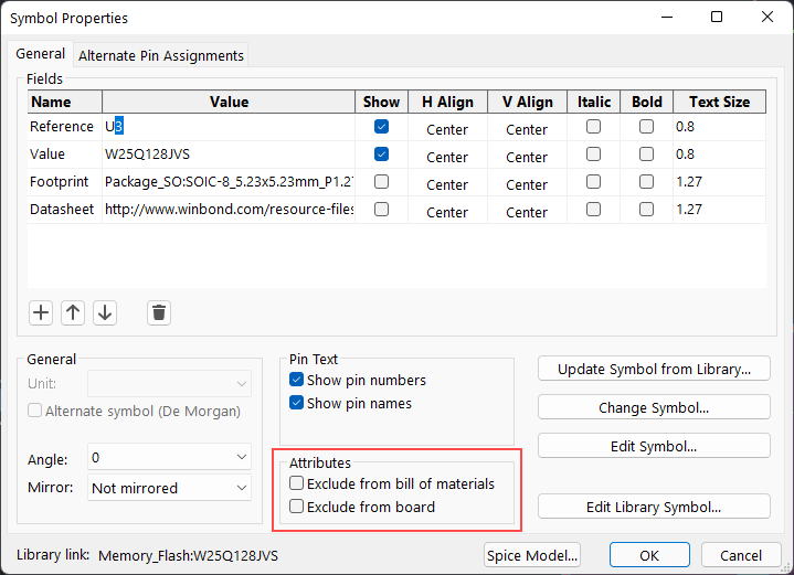
Bill of Materials (BoM) is the complete list of parts with reference designators, component value, package, quantity, and Manufacturer Part Number (MPN). You must use a spreadsheet file for BoM. Other file types are not easily editable by the assembly house. If you’re using Turnkey service, the assembly house will fill in the cost and other details for you to review. When you do not want to assemble certain components, you can exclude them from the BoM or add a Do Not Place (DNP) label or you can use the Exclude from bill of materials option from component properties in KiCad.
Do not add any components to the BoM, that can’t be soldered, such as virtual parts. Carefully check your BoM before sending. Your BoM must be consistent with all other files. For example, if you have a component named R5, the value and number should be the same in fab layers, silkscreen, and assembly drawings. Sometimes manufacturers will provide a spreadsheet template that you can use as a reference. Usually, it looks like this,
| Sl. No. | Reference | Value | Description | Package | Quantity | MPN | Notes |
|---|---|---|---|---|---|---|---|
| Sequence Number | Designators | Component Value | Specifications | SMD/THT Packages | Required quantity | Manufacturer Part Number | Extra notes |
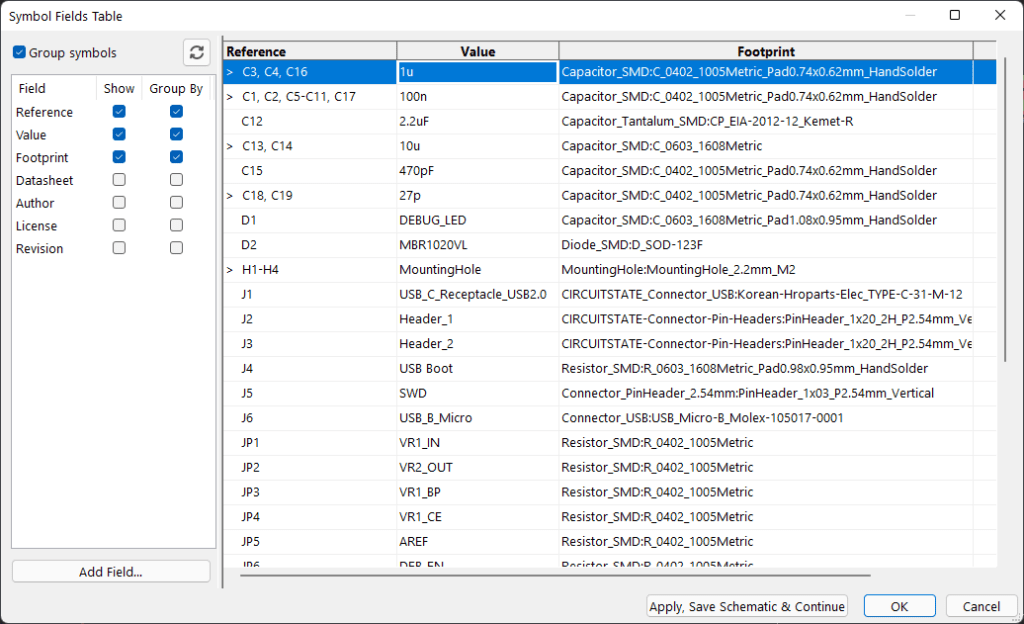
The manufacturer will then add extra columns such as unit price, quantity price, MOQ, etc. It is also advised to add distributor part numbers such as those used by Mouser, DigiKey, LCSC, etc. The description must give the most important specifications of the part. For example, 120K, 1%, 0603 chip resistor for an SMD resistor. You can also add alternate MPNs to allow the assembly house to choose the one with the most availability and less cost. If you start using the actual values and MPNs even from the start of the design, a lot of headaches can be avoided later. In KiCad, you can use the bulk editing of symbol tables feature for adding them.
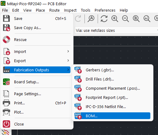
Once you have edited all the component properties, you can export the BoM from File → Fabrication Outputs → BoM. This file will be in CSV (Comma Separated Values) format, with a semicolon as a separator. CSV file can be imported to an Excel sheet by choosing a semicolon as the separator. Each item on a row separated with a semicolon will get a separate column.
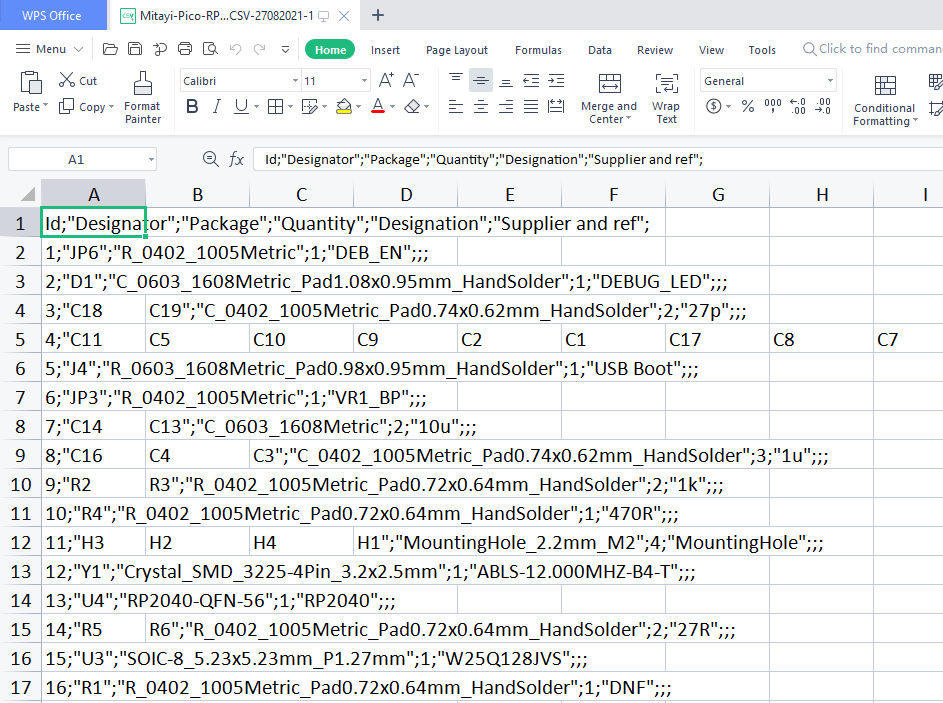
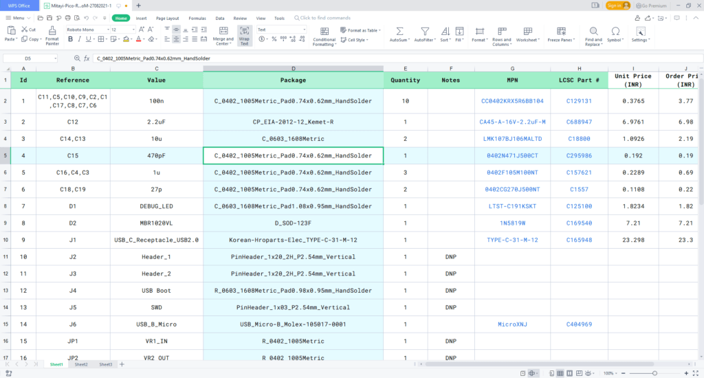
Once you have exported the BoM, you can use any BoM scrubbing and sourcing tool to find available parts and order them. oemsecrets.com is such a tool where you can upload your BoM and find parts from leading suppliers such as Mouser and DigiKey. LCSC also has a BoM scrubbing tool which works great.
Additionally, you can create a beautiful HTML-based interactive BoM with the help of this open-source plugin (developed by Open Scope Project) for KiCad. This can be a great help for manual assembly.
Position Files
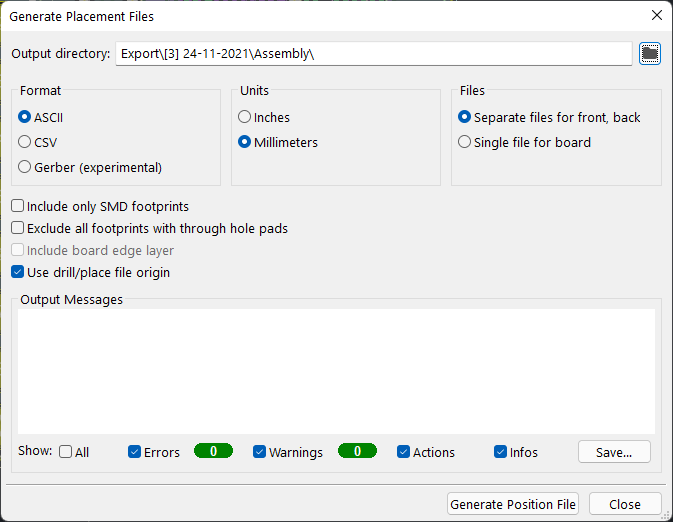
The position file contains the list of all component designators and their positions on the PCB. A position file is also called an XY file or Centroid or Placement file. See the position file exported for the Mitayi project below. This is the ASCII version with separate files for the top and bottom sides, and uses drill origin as board origin.
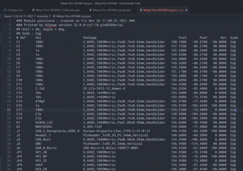
You might wonder where these XY coordinates are coming from. Every component has to have an origin set somewhere, that is possible for a Pick and Place (PnP) machine to pick it up from. This location will be usually specified in the datasheet of the part. Otherwise, the center of the component is used as the origin. One has to follow instructions in the datasheet when creating a new footprint. But not everyone does this right and that can cause issues when you are using the footprint for PCBA. If you downloaded a footprint from the web, it will be better to check if they have these pickup locations set correctly. In KiCad, these origin points will appear as anchor points as seen as a green + symbol below. It is this coordinate value that appears in the position file. If the pickup location is hard to show in the files, you can show it on the assembly drawing.
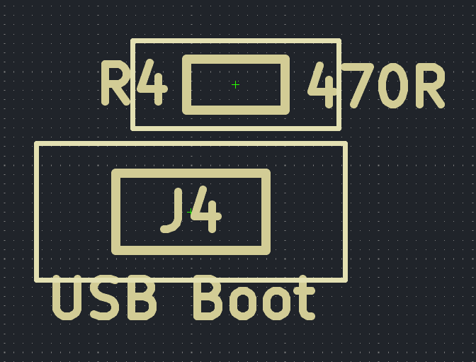
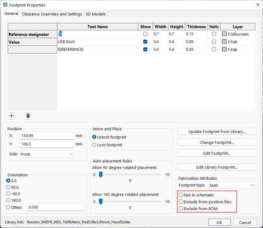
Another thing to keep in mind is the rotation of each component. If a component footprint is designed the correct way, KiCad will take care of the rotation value. But if it is not, you will have to manually adjust them. If you want to exclude a footprint from the position files, you can do so by opening the footprint properties and then marking the checkbox Exclude from position files. Position files can be exported from the same File → Fabrication Outputs menu in KiCad.
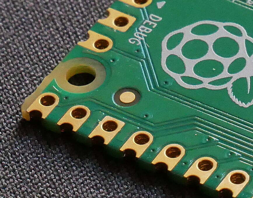
Fiducials are free pads, usually circular in shape, that are placed on the PCB to optically determine the orientation of a PCB. The latest machines do not require fiducials but it’s a good practice to add them if you have enough space. Since fiducials have to indicate incorrect orientation, they are placed in an asymmetrical way. This means, that if you flip or rotate the board, the fiducials on the board will no longer align with a reference image. The fiducials can be placed during panelization, on the outside of the PCB, or can be placed on individual PCBs. Fiducials can also help identify the orientation in assembly drawings.
Assembly Drawing
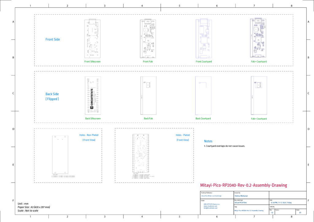
Assembly drawing is the visual representation of your PCB, that shows component designators, values, and other markings. KiCad does not have the option to export assembly drawings directly but they can be created from exported PDF files. You can export your PCB layers as PDFs using the Plot dialog seen below. Make sure you select all the layers required.
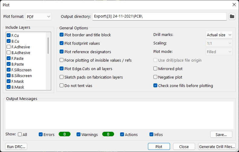
Choose PDF as the plot format. We also need to keep the page border, title block, and board outline on all pages. If you keep the drill marks to actual sizes, holes will be created on all layers where the drill is applicable. For example, if you have text placed on a via, the drill mark will clip the text on the exported PDF. This can make reading the text, especially smaller ones, difficult to read. Keep all other settings as above. All layers will be exported as individual PDF files. These PDF files can be opened in any vector editing software and be combined into a single page. We usually use A4 or A3 in landscape mode for assembly drawings. Graphical layers to include in assembly drawing are,
- Board outline
- Silkscreen
- Fabrication layers
- Courtyard layers
- Dimensions
- Drills and Holes
Use consistent orientations for all graphics with a scale of 1:1 even though the drawings are not for actual machining. Include extra information if there is any, such as how to solder wires or insert certain connectors. This information will be used by human operators rather than machines. Below is the assembly drawing for Mitayi Pico RP2040. You can use our PDF as a template.
3D Files
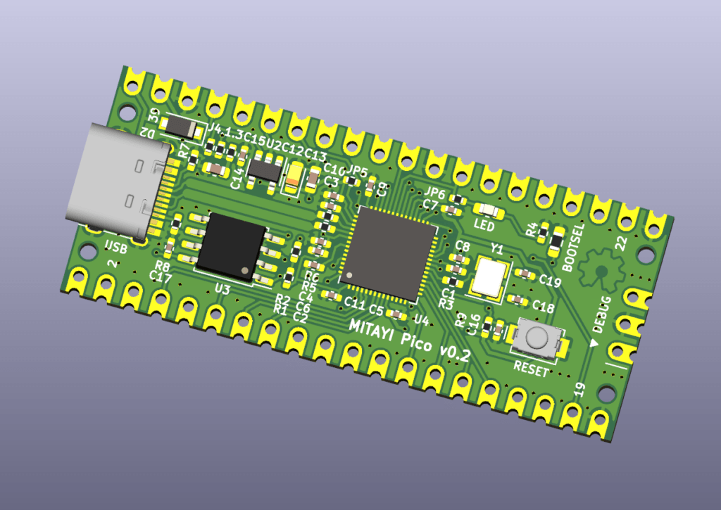
Nothing else is better than an actual 3D model of your board with all the components populated. This is usually not necessary but can be included as extra information. KiCad can export entire PCBs as a STEP file suitable for viewing in most 3D CAD software. Unfortunately, KiCad does not export the silkscreen or copper layers in a 3D file. But you can also send the 3D render or the screenshot taken from KiCad’s 3D viewer.
Sourcing Components
Sourcing components can be a surprisingly difficult task depending on the type of components, cost, region, and quantity required. There are three ways you can source components for your PCBA project.
- Turnkey – this is where you give a complete list of parts to the assembly house and they will procure all the parts for you. Some manufacturers stock the widely used parts in their warehouses. They can also combine our parts with other orders and thus get a high volume price reduction. If the assembly house is located in proximity to large industrial cities, that can also reduce procuring time and cost.
- Consigned/Kitted – this is when you provide all the components directly to the assembly house, either because you are producing the parts or you already have a stock of the parts required. The components must have packaging suitable for automatic feeding.
- Combination or Partially Consigned – this is when you have some of the components in stock but the remaining has to be purchased. This happens when you have stock of rare-to-find parts but everything else is general purpose.
Keep the following things in mind when you are sourcing components for assembly.
- Choose parts with long production life, high availability, low cost, and availability of alternatives. If you choose obsolete or rare-to-find parts, it can lead to a production halt at some point after the production has begun.
- Reserve the parts even before you complete your design, if possible. If any components go out of stock by the time you finish your design, you might end up having to redesign your project.
- Have a list of alternative parts in your BoM and add design provisions that will allow supporting different parts without changing the design. Usually, this can be accomplished by using solder jumpers and small tweaking of footprints.
- Create an accurate Bill of Materials (BoM) that is consistent with all other files.
- Make sure components are properly packed in their original packaging. For example, some components are susceptible to humidity and will require baking before they can be used for assembly. Humidity exposure can be tracked with humidity indicator cards. If the parts are not packed properly, this can lead to assembly issues later. Follow the manufacturer’s guidelines for packaging and handling.

Single or Double Side Assembly
Boards can have components on both sides or on a single side. Not all manufacturers provide double-sided assembly. Check with the assembly house whether they support double-side assembly.
Reflow Profiles
If your board is going to be soldered by a reflow oven, then specific reflow profiles have to be followed for your PCBs. Usually, the assembly house will take care of this depending on what type of components you have, the type of solder used, and the process used. Component datasheets will also have specific reflow profiles to be followed. If you have special types of parts in your design that require special attention, make sure you communicate it with the assembly house.
Stencil
A stencil is a masking material made of a thin steel sheet. This is used for applying solder paste on the board. Stencils can be created for individual PCBs or a PCB panel. The stencil is created by laser cutting with the information from the solder paste layer. Sometimes the assembly house will charge extra for creating stencils and they might even ship it with your PCBs. Ask your assembly house whether they charge for or send stencils.
Sending to Assembly House
Sending the files to the assembly house is similar to how we do it for PCB fabrication. You can ZIP all the files and send them for review. Depending on how you are sourcing the parts, you have to manage the payment and logistics. PCBWay has given a list of requirements when sending the parts. If there are any issues in the files, most assembly houses will help you to rectify them. Assembly houses estimate the assembly cost based on many parameters such as how many components you have, single side or double side, type of PCB, the complexity of soldering, the sensitivity of components, etc. Let’s see how you can send an assembly quote to PCBWay through their web interface. First, go to the order quote page.
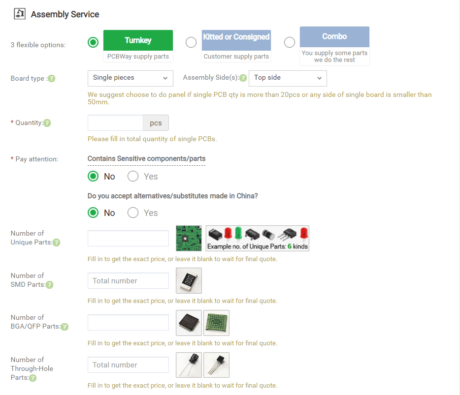
If you are not yet sure about how many components you have, you can leave it blank and later submit the complete BoM for assembly. One of PCBWay’s representatives will check your BoM and update you on the total cost. PCBWay can source parts from all major distributors including Mouser, DigiKey, and LCSC, and even use compatible alternatives they have already in stock. Components like resistors and capacitors will fall into this category.
PCBWay also suggests you panelize the PCBs if there is more quantity and you can receive either assembled PCB panels or depanelized single PCBs. Such special requirements can be specified in the Additional Options section. Additionally, you can ask PCBWay to upload the firmware to test the functionality of the boards after assembly. This can make sure that the assembled PCBs are functional before being shipped. Conformal coating is an insulating layer that protects the PCBs from oxidation, moisture, and other contaminants. You can always bundle an assembly order with a PCB order and vice versa.

PCB Inspection
A good service provider will run your PCBs through various test procedures to make sure the assembled PCBs meet the required quality specifications. You can request the assembly house to provide the test reports of your PCBs.
That’s all for this tutorial. Let us know if we missed something or ways to improve this article.
Links
- Download KiCad
- Generate Gerber files from KiCad
- Order PCBs at PCBWay
- Place PCBA order at PCBWay
- SMT PCB assembly ordering guide – PCBWay
- KiCad PCB Panelizing Plugin
- KiCad Interactive HTML BoM Plugin
- BoM Scrubbing and Sourcing Tool – Oemsecrets.com
Short Link
- Short URL to this page – https://circuitstate.com/kicadtopcba
