Blinking LED with Timer Interrupts : Learn Microcontroller with STM8S – Tutorial Part #5
Learn how to blink an LED with microcontroller timers and interrupts. Generate precise timing by programming the built-in timers of STM8S.
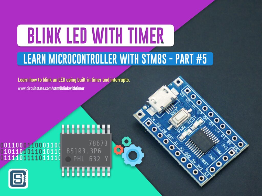
In the last tutorial, we learned how to use the GPIO pin to control an LED. In that we used the instruction cycle lengths to generate the timing we need. Generating precise timing in that way can be difficult for practical applications. That is why we have dedicated digital Timers/Counters built into modern microcontrollers. STM8S also have powerful timers that can be easily programmed by the user. In this tutorial, we will learn how to blink the same LED but now with the timing generated from programmable timers. We will also use our first interrupt-enabled program. If you missed the previous part of this tutorial series, you can find it below for reading.
Wiring Up & Writing Your First Blink Program Using Assembly Language : Learn Microcontroller with STM8S – Tutorial Part #4
Tutorial Series
- Learn the fundamentals of microcontrollers.
- Familiarize with a simple STM8S microcontroller.
- Install all the software tools and prepare your computer for programming and debugging microcontrollers.
- Get hands on experience with connecting your first microcontroller board and write a program for it.
- Learn the concepts of timers and interrupts in microcontrollers and blink an LED with what you learn.
- Learn how to make your microcontroller interact with the world by reading a push-button.
- Learn how to read a push-button using external interrupts without blocking critical code.
- Learn how to use the UART peripheral to print your first “Hello World” message to a computer.
What You’ll Learn
- Learn about software interrupts.
- Learn about timers and counters in STM8S.
- Learn how to use timer interrupts in an Assembly program.
Interrupts
Interrupts are interesting concept in computing and it makes computers practical. We will use an example to show how interrupts are useful. Say you are a baker with two jobs, one is to constantly make new cakes and the second one is to pack cakes when a customer comes to your shop and place an order. You are the only one in the shop and so you have to do both. Now, if there are no orders pending, you can keep making cakes without stopping. But if a customer comes up and ask for a cake, you have to stop making cakes temporarily and start packing the cakes for the customer. So if you are packing cakes, you can not make cakes. You can only do one thing at a time.
Now the problem is, you do not know when a customer is going to come up to your shop and place an order. If you simply wait for customers, you won’t be able to make cakes in the first place. If you only focus on making cakes, and don’t attend to the customers, you will never sell any cakes. So what’s the solution? You can continue making cakes as long as there are no orders pending and whenever you do get an order, you can pause making cakes and start packing them instead. Since you can not predict when you are going to get an order, such an event is called an Asynchronous event. Many events in practical life are asynchronous in nature. Computers will also need to deal with them and they do it through an interrupt logic.
Computer interrupts are events that are not predictable in time (when they happen), but predictable in type. Interrupts temporarily stops the main logic of a program and divert the logic to a subroutine which is normally called an Interrupt Service Routine (ISR). ISR is a function that is part of the main code but it is not executed in normal operation. ISRs are only called when their corresponding interrupt occurs. For example, one type of interrupt supported by the STM8 microcontroller is the GPIO input interrupt. It allows a GPIO pin to be configured as input and wait for an interrupt to happen. The interrupt functionality can be enabled from the Px_CR2 register. We will explain more about interrupts in the next tutorial.
There are Maskable interrupts and Non-maskable interrupts. Maskable interrupts are interrupts that can be disabled by the programmer. These are usually low priority interrupts that are not critical. Non-maskable interrupts are critical interrupts that can not be disabled. RESET, TRAP and TLI are the non-maskable interrupts in STM8S. The interrupts are managed by a special logical block called the Interrupt Controller (ITC) and it has the following features.
- Management of hardware interrupts:
– External interrupt capability on most I/O pins with dedicated interrupt vector and edge sensitivity setting per port
– Peripheral interrupt capability - Management of software interrupt (
TRAP) - Nested or concurrent interrupt management with flexible interrupt priority and level management:
– Up to 4 software programmable nesting levels
– Up to 32 interrupt vectors fixed by hardware
– 2 non maskable events:RESET,TRAP
– 1 non-maskable top level hardware interrupt (TLI)
This interrupt management is based on: - Bit
I1andI0of the CPU Condition Code register (CCR) - Software priority registers (
ITC_SPRx) - Reset vector address
0x00 8000at the beginning of program memory. In devices with boot ROM, the reset initialization routine is programmed in ROM by STMicroelectronics. - Fixed interrupt vector addresses located at the high addresses of the memory map (
0x00 8004to0x00 807C) sorted by hardware priority order.
Interrupt Management
What explained in this section can be a little too much to take in first. If you feel like not understanding everything, try skipping this section and instead see everything in action first. Then later, you can revisit this section to pick up what you need to know. We will also limit the details to an overall minimum. If you need to understand everything in detail, check out Chapter 6, Interrupt Controller, in the RM0016 – STM8S and STM8AF Series 8-Bit Microcontrollers document.
The interrupts in the STM8S microcontroller are managed by the ITC as said earlier. The ITC supports multiple priorities for the interrupts. That means, a higher priority ISR can actually interrupt a lower priority ISR. This results in the nested interrupts capability. Interrupt masking (preventing an interrupt from firing) and priorities are managed by the I1 and I0 bits in the CC register as well as the software priority registers ITC_SPRx. When an interrupt occurs, the following things happen.
- Normal processing is suspended at the end of the current instruction execution.
- The
PC,X,Y,AandCCRregisters are saved onto the stack. - Bits
I1andI0ofCCRregister are set according to the values in theITC_SPRxregisters corresponding to the serviced interrupt vector. - The
PCis then loaded with the interrupt vector of the interrupt to service and the first instruction of the interrupt service routine is fetched. - After the ISR is complete, the instruction
IRETcauses the saved registers to be restored from the stack and normal (even a nested ISR) execution resumes.
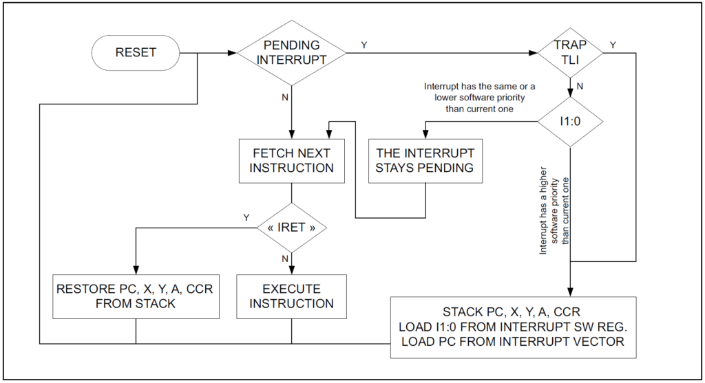
Following is the interrupt priority levels in STM8S.

As you can see there can be four interrupt priority levels. When the ITC is in the lowest priority mode, all supported interrupts are enabled and can be serviced. As the priority level is increased, lower priority interrupts are disabled. In the highest priority mode, all software interrupts are disabled and only the hardware interrupts are served. If you are wondering what are all the interrupts supported here, following is a list of all of the interrupt vectors.
| IRQ # | Source Block | Description | Wakeup from Halt mode | Wakeup from Active-Halt mode | Vector Address |
|---|---|---|---|---|---|
| – | RESET | Reset | Yes | Yes | 0x00 8000 |
| – | TRAP | Software interrupt | – | – | 0x00 8004 |
| 0 | TLI | External top level interrupt | – | – | 0x00 8008 |
| 1 | AWU | Auto wake up from halt | – | Yes | 0x00 800C |
| 2 | CLK | Clock controller | – | – | 0x00 8010 |
| 3 | EXTI0 | Port A external interrupts | Yes ¹ | Yes ¹ | 0x00 8014 |
| 4 | EXTI1 | Port B external interrupts | Yes | Yes | 0x00 8018 |
| 5 | EXTI2 | Port C external interrupts | Yes | Yes | 0x00 801C |
| 6 | EXTI3 | Port D external interrupts | Yes | Yes | 0x00 8020 |
| 7 | EXTI4 | Port E external interrupts | Yes | Yes | 0x00 8024 |
| 8 | Reserved | – | – | – | 0x00 8028 |
| 9 | Reserved | – | – | – | 0x00 802C |
| 10 | SPI | End of transfer | Yes | Yes | 0x00 8030 |
| 11 | TIM1 | TIM1 update/ overflow/ underflow/ trigger/ break | – | – | 0x00 8034 |
| 12 | TIM1 | TIM1 capture/ compare | – | – | 0x00 8038 |
| 13 | TIM2 | TIM2 update/ overflow | – | – | 0x00 803C |
| 14 | TIM2 | TIM2 capture/ compare | – | – | 0x00 8040 |
| 15 | Reserved | – | – | – | 0x00 8044 |
| 16 | Reserved | – | – | – | 0x00 8048 |
| 17 | UART1 | Tx complete | – | – | 0x00 804C |
| 18 | UART1 | Receive register DATA FULL | – | – | 0x00 8050 |
| 19 | I2C | I2C interrupt | Yes | Yes | 0x00 8054 |
| 20 | Reserved | – | – | – | 0x00 8058 |
| 21 | Reserved | – | – | – | 0x00 805C |
| 22 | ADC1 | ADC1 end of conversion/ analog watchdog interrupt | – | – | 0x00 8060 |
| 23 | TIM4 | TIM4 update/ overflow | – | – | 0x00 8064 |
| 24 | Flash | EOP/WR_PG_DIS | – | – | 0x00 8068 |
| Reserved | 0x00 806C to 0x00 807C |
That makes 32 of them. Among these, the first three are exclusive hardware interrupts and they will be served regardless of the state of the I1 and I0 bits. That means, when I1 and I0 are 11, only RESET, TRAP and TLI are served. Everything else is disabled. The priorities of the remaining software interrupts can be programmed via the corresponding ITC_SPRx register. Following is a list of all of them.
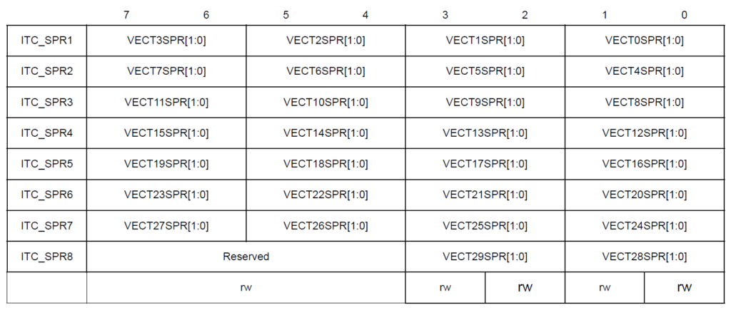
Following is the interrupt priority decision process.
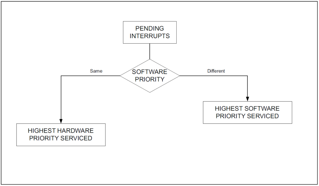
Timer
A Timer inside a microcontroller is actually a Digital Counter. A digital counter can count the number of times the state of its input changes. You can use, for example, a square wave signal as the input to a counter and each time a transition occurs, the value of the counter advances by one. This is best demonstrated in the following animation.
A counter value is usually reset to 0 before starting. Each time a LOW to HIGH transition (Rising Edge) occurs, the counter advances its value by 1. Since a rising edge only occurs after each complete cycle of a square wave, the counter will essentially be counting the pulses. If we reset the counter after every 1 second, we will count the frequency of the square wave, which is how most of the frequency counters work. If we can measure the frequency of a signal, we can also calculate the time period. But this requires a reference timing event. One of the easiest to find a timing reference in a microcontroller systems is the Crystal oscillator circuit. Quartz crystals are very precise in generating clock signals for microprocessors. If we know the frequency of the crystal, we can calculate the time period. For example, the 16 MHz clock of the STM8 microcontroller has a time period of,
Cycle Period = 1 / (16 x 106) = 62.5 ns (62.5 x 10⁻⁹ S)
That means, the time between a rising edge to the next rising edge is around 62.5 nanoseconds. Now we can start understanding the Timers and Counters inside the STM8 microcontroller. Microcontrollers in the STM8S family can have up to three different types of timers.
- Advanced Timers – 16-bit timer denoted as
TIM1. - General Purpose Timers – 16-bit timers denoted as
TIM2,TIM3orTIM5. - Basic Timers – 8-bit timers denoted as
TIM4orTIM6.
The STM8S103F3 on the STM8S-Blue board has the following timers.
- 1 x Advanced Timer –
TIM1(16-bit) - 1 x General Purpose Timer –
TIM2(16-bit) - 1 x Basic Timer –
TIM4(8-bit)
Following are the timer characteristics in STM8. We will explain all of them further down.

Following is the comparison between the different types of timers and what makes them different.
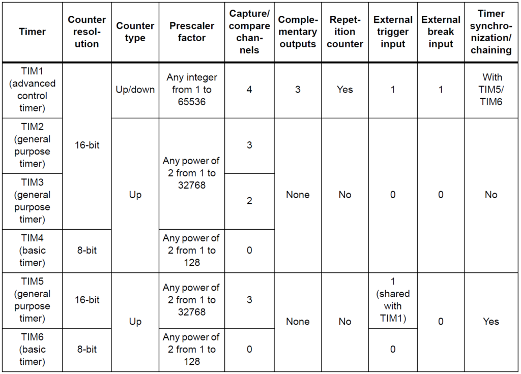
The resolution of a timer is the maximum size of the counter. For example a 16-bit timer has a 16-bit counter value and can count from 0 to 65535, which is a total of 65536 counts. An 8-bit timer on the other hand, can only count up to 255 (256 counts). After the maximum count is reached, the counter has to be reset to 0 or some other value. The higher the resolution a timer has, the better will be the time precision.
Counters can count up or down. This simply refers to how the counter value is changed for each input. If the value is incremented for each pulse input, it is called an Up Counter. If the value is decremented for each input, it is called a Down Counter. Counters that supports both up and down function can be programmed for the type of counting.
A Capture Mode in a timer is how it detects the presence of a pulse or an event. This can be programmed to be different events such as rising edge, falling edge, every fourth rising edge etc. Compare Mode in timer is a special operation that triggers an action when the captured count matches a preset value. For example, we can program the compare value to 16 and wait for that many pulses to be counted before an action is triggered.
We are first going to use the only general purpose timer the STM8 has; TIM2. Following are the features of the TIM2.
- 16-bit up counting auto-reload counter.
- 4-bit programmable prescaler allowing the counter clock frequency to be divided “on
the fly” by any power of 2 from 1 to 32768. - 3 independent channels for:
– Input capture
– Output compare
– PWM generation (edge-aligned mode) - Interrupt request generation on the following events:
– Update: counter overflow, counter initialization (by software)
– Input capture
– Output compare
Following is the block diagram of TIM2.
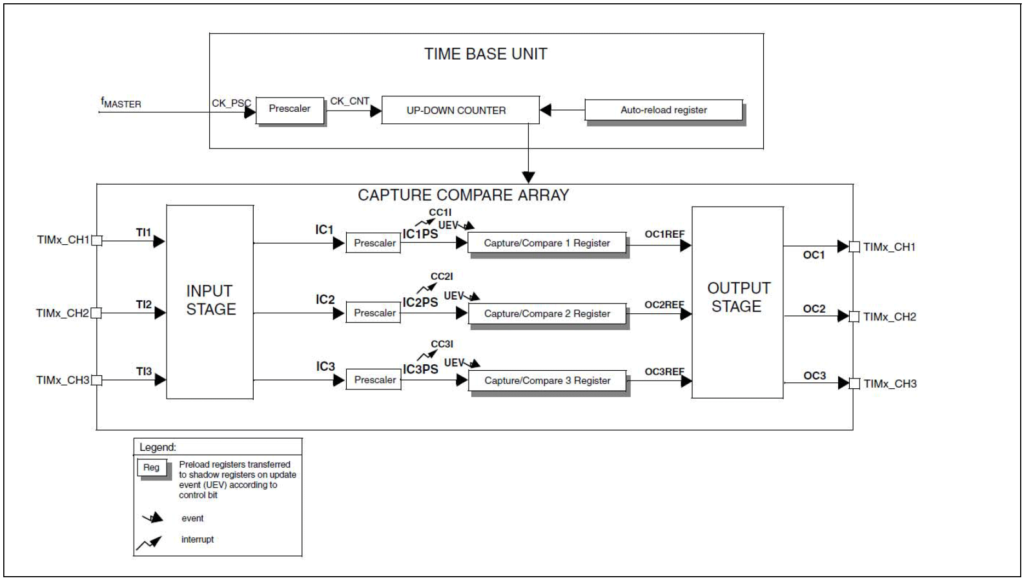
fMASTER is the internal input clock for the timer. This is a square wave signal that acts as a reference clock signal for the timer. A Prescaler is a value by which you can divide the input signal. For example, if the master frequency is 10 Hz and we want to divide the signal by 2, we can load the prescaler with 2 and it will produce 5 Hz at the output. How, you are wondering? The prescaler is a counter itself, that counts the input pulses and only produce an output pulse when the input pulse count matches the prescaler value. So each time the prescaler counter counts 2 pulses, it produces a single output pulse. This essentially divides the master clock by two.
An Auto-reload Register is a memory location where you can save a value, which will be loaded to the main counter register when it overflows. We will see how this feature is used in our example program.
Apart from the internal master clock, the timers/counters can also count external pulses using the capture/compare blocks. The inputs of the timers will be tied to multiple GPIO pins for this. Each such input is called a channel of the timer. Similarly, GPIO pins can also be used to output signals from the timers. These are also called channels. The timer we are going to use, TIM2 has three independent channels that can be used as either input or output. As you can also see from the block diagram, timers can also generate different interrupts.
Blink with Timer
The functions of a timer is best explained with an example program. The Blink program we last used will be rewritten to use a timer interrupt to generate accurate delay between switching the LED on and off. So instead of using NOP instruction to “waste” the time of the CPU, it can perform something useful while the timer takes care of timing. Let’s start with the code.
Code
.stm8

; STM8 assembler demo:
; LED blinking on a timer interrupt
; Version 0.1

; LED pin index on Port B
LED     EQU     5

; Code start
.org 0x8080

.include "stm8s103.inc"

; Main program body
start:
    SIM                         ; Disable interrupts
    BSET    PB_DDR, #LED        ; Set the LED pin as output
    BSET    PB_CR1, #LED        ; Set the LED pin as push-pull

    MOV     TIM2_ARRH, #0x7A    ; Set the auto-reload value to 31250
    MOV     TIM2_ARRL, #0x12    ; which should give us the interrupt interval of:
                                ; 1 / (2000000 / 32 / 31250) = 0.5 s
    MOV     TIM2_PSCR, #5       ; Set the prescaler to divide the clock by 32
    BSET    TIM2_IER, #0        ; Enable update interrupt
    RIM                         ; Enable interrupts

    BSET    TIM2_CR1, #0        ; Enable the timer

loop:
    WFI                         ; wait for an interrupt
    JP      loop                ; loop forever

; TIM2 update/overflow handler
.func tim2_overflow
    BCPL    PB_ODR, #LED        ; Toggle the LED pin
    BRES    TIM2_SR1, #0        ; Reset timer's update interrupt flag
    IRET
.endf

; Interrupt vectors
.org 0x8000
    INT     start                   ; RESET handler, jump to the main program body

.org 0x803c
INT tim2_overflow ; IRQ13: TIM2 update/overflow interruptCode Explained
Only new features or instructions will be explained from here on. Instructions that are covered in the previous examples are not explained again. We hope that you still recall the instructions we have already learned and if you have any doubts, feel free to check the previous examples.
.include "stm8s103.inc"This line uses the .include directive to include an external assembly file containing all of the constant symbols. Yes, we can split a large program into smaller and reusable chunks and ask the Assembler to combine them. The file stm8s103.inc contains a few extra directives that describes the features of the specific microcontroller we are using. It has the following contents.
; vim: ft=asm
.stm8

; MCU family selection
.define STM8S103
.define STM8_ACCESS_LINE
.define STM8_LOW_DENSITY

; Optional peripherals
.define STM8_HAS_ADC1
.define STM8_HAS_BEEP
.define STM8_HAS_TIM2
.define STM8_HAS_TIM4
.define STM8_HAS_UART1

.include "stm8s.inc".define is a new Assembler directive that creates a constant value. When a value is defined, you can add a value or an expression. It is also used to check the presence of features. The usage is similar to the #define macro in C/C++ language. Here we are using the macros to define a features supported by the STM8S103 series microcontrollers.
At the end of the file, you also see the inclusion of another file. And yes, you can nest the include files like that. So when you add the stm8s103.inc file to your main code, the stm8s.inc is automatically included. Such file inclusions are referred to as nested dependencies. The stm8s.inc file has a long list of macros.
; vim: ft=asm
.stm8

;
; Common memory layout definitions
;
RAM_START       equ 0x0000
EEPROM_START    equ 0x4000
ROM_START       equ 0x8000
; Interrupt vectors occupy first 128 bytes of Flash
VECTORS_START   equ 0x8000
; Code/data sections starts just after the vectors
CODE_START      equ 0x8080

;
; Unique ID
;
U_ID        equ 0x4865      ; Unique ID (96-bits)
U_ID_SIZE   equ (96 / 8)    ; Length of the UID

;
; GPIO
;
PA_ODR      equ 0x5000 ; Port A data output latch register
PA_IDR      equ 0x5001 ; Port A input pin value register
PA_DDR      equ 0x5002 ; Port A data direction register
PA_CR1      equ 0x5003 ; Port A control register 1
PA_CR2      equ 0x5004 ; Port A control register 2

PB_ODR      equ 0x5005 ; Port B data output latch register
PB_IDR      equ 0x5006 ; Port B input pin value register
PB_DDR      equ 0x5007 ; Port B data direction register
PB_CR1      equ 0x5008 ; Port B control register 1
PB_CR2      equ 0x5009 ; Port B control register 2

PC_ODR      equ 0x500A ; Port C data output latch register
PC_IDR      equ 0x500B ; Port C input pin value register
PC_DDR      equ 0x500C ; Port C data direction register
PC_CR1      equ 0x500D ; Port C control register 1
PC_CR2      equ 0x500E ; Port C control register 2

PD_ODR      equ 0x500F ; Port D data output latch register
PD_IDR      equ 0x5010 ; Port D input pin value register
PD_DDR      equ 0x5011 ; Port D data direction register
PD_CR1      equ 0x5012 ; Port D control register 1
PD_CR2      equ 0x5013 ; Port D control register 2

PE_ODR      equ 0x5014 ; Port E data output latch register
PE_IDR      equ 0x5015 ; Port E input pin value register
PE_DDR      equ 0x5016 ; Port E data direction register
PE_CR1      equ 0x5017 ; Port E control register 1
PE_CR2      equ 0x5018 ; Port E control register 2

PF_ODR      equ 0x5019 ; Port F data output latch register
PF_IDR      equ 0x501A ; Port F input pin value register
PF_DDR      equ 0x501B ; Port F data direction register
PF_CR1      equ 0x501C ; Port F control register 1
PF_CR2      equ 0x501D ; Port F control register 2
.ifdef STM8_HAS_PORT_G
PG_ODR      equ 0x501E ; Port G data output latch register
PG_IDR      equ 0x501F ; Port G input pin value register
PG_DDR      equ 0x5020 ; Port G data direction register
PG_CR1      equ 0x5021 ; Port G control register 1
PG_CR2      equ 0x5022 ; Port G control register 2
.endif
.ifdef STM8_HAS_PORT_H
PH_ODR      equ 0x5023 ; Port H data output latch register
PH_IDR      equ 0x5024 ; Port H input pin value register
PH_DDR      equ 0x5025 ; Port H data direction register
PH_CR1      equ 0x5026 ; Port H control register 1
PH_CR2      equ 0x5027 ; Port H control register 2
.endif
.ifdef STM8_HAS_PORT_I
PI_ODR      equ 0x5028 ; Port I data output latch register
PI_IDR      equ 0x5029 ; Port I input pin value register
PI_DDR      equ 0x502A ; Port I data direction register
PI_CR1      equ 0x502B ; Port I control register 1
PI_CR2      equ 0x502C ; Port I control register 2
.endif

;
; FLASH
;
FLASH_CR1   equ 0x505A ; Flash control register 1
FLASH_CR2   equ 0x505B ; Flash control register 2
FLASH_NCR2  equ 0x505C ; Flash complementary control register 2
FLASH_FPR   equ 0x505D ; Flash protection register
FLASH_NFPR  equ 0x505E ; Flash complementary protection register
FLASH_IAPSR equ 0x505F ; Flash in-application programming status register
FLASH_PUKR  equ 0x5062 ; Flash program memory unprotection register
FLASH_DUKR  equ 0x5064 ; Data EEPROM unprotection register

;
; ITC
;
EXTI_CR1    equ 0x50A0 ; External interrupt control register 1
EXTI_CR2    equ 0x50A1 ; External interrupt control register 2

;
; RST
;
RST_SR      equ 0x50B3 ; Reset status register

;
; CLK
;
CLK_ICKR        equ 0x50C0 ; Internal clock control register
CLK_ECKR        equ 0x50C1 ; External clock control register
CLK_CMSR        equ 0x50C3 ; Clock master status register
CLK_SWR         equ 0x50C4 ; Clock master switch register
CLK_SWCR        equ 0x50C5 ; Clock switch control register
CLK_CKDIVR      equ 0x50C6 ; Clock divider register
CLK_PCKENR1     equ 0x50C7 ; Peripheral clock gating register 1
CLK_CSSR        equ 0x50C8 ; Clock security system register
CLK_CCOR        equ 0x50C9 ; Configurable clock control register
CLK_PCKENR2     equ 0x50CA ; Peripheral clock gating register 2
.ifdef STM8_HAS_CAN
CLK_CANCCR      equ 0x50CB ; CAN clock control register
.endif
CLK_HSITRIMR    equ 0x50CC ; HSI clock calibration trimming register
CLK_SWIMCCR     equ 0x50CD ; SWIM clock control register

;
; WWDG
;
WWDG_CR     equ 0x50D1 ; WWDG control register
WWDG_WR     equ 0x50D2 ; WWDG window register

;
; IWDG
;
IWDG_KR     equ 0x50E0 ; IWDG key register
IWDG_PR     equ 0x50E1 ; IWDG prescaler register
IWDG_RLR    equ 0x50E2 ; IWDG reload register

;
; AWU
;
AWU_CSR     equ 0x50F0 ; AWU control/status register 1
AWU_APR     equ 0x50F1 ; AWU asynchronous prescaler buffer register
AWU_TBR     equ 0x50F2 ; AWU timebase selection register

;
; BEEP
;
.ifdef STM8_HAS_BEEP
BEEP_CSR    equ 0x50F3 ; BEEP control/status register
.endif

;
; SPI
;
SPI_CR1     equ 0x5200 ; SPI control register 1
SPI_CR2     equ 0x5201 ; SPI control register 2
SPI_ICR     equ 0x5202 ; SPI interrupt control register
SPI_SR      equ 0x5203 ; SPI status register
SPI_DR      equ 0x5204 ; SPI data register
SPI_CRCPR   equ 0x5205 ; SPI CRC polynomial register
SPI_RXCRCR  equ 0x5206 ; SPI Rx CRC register
SPI_TXCRCR  equ 0x5207 ; SPI Tx CRC register

;
; I2C
;
I2C_CR1     equ 0x5210 ; I2C control register 1
I2C_CR2     equ 0x5211 ; I2C control register 2
I2C_FREQR   equ 0x5212 ; I2C frequency register
I2C_OARL    equ 0x5213 ; I2C own address register low
I2C_OARH    equ 0x5214 ; I2C own address register high
I2C_DR      equ 0x5216 ; I2C data register
I2C_SR1     equ 0x5217 ; I2C status register 1
I2C_SR2     equ 0x5218 ; I2C status register 2
I2C_SR3     equ 0x5219 ; I2C status register 3
I2C_ITR     equ 0x521A ; I2C interrupt control register
I2C_CCRL    equ 0x521B ; I2C clock control register low
I2C_CCRH    equ 0x521C ; I2C clock control register high
I2C_TRISER  equ 0x521D ; I2C TRISE registerr
I2C_PECR    equ 0x521E ; I2C packet error checking register

;
; UART1
;
.ifdef STM8_HAS_UART1
UART1_SR    equ 0x5230 ; UART1 status register
UART1_DR    equ 0x5231 ; UART1 data register
UART1_BRR1  equ 0x5232 ; UART1 baud rate register 1
UART1_BRR2  equ 0x5233 ; UART1 baud rate register 2
UART1_CR1   equ 0x5234 ; UART1 control register 1
UART1_CR2   equ 0x5235 ; UART1 control register 2
UART1_CR3   equ 0x5236 ; UART1 control register 3
UART1_CR4   equ 0x5237 ; UART1 control register 4
UART1_CR5   equ 0x5238 ; UART1 control register 5
UART1_GTR   equ 0x5239 ; UART1 guard time register
UART1_PSCR  equ 0x523A ; UART1 prescaler register
.endif

;
; UART2
;
.ifdef STM8_HAS_UART2
UART2_SR    equ 0x5240 ; UART2 status register
UART2_DR    equ 0x5241 ; UART2 data register
UART2_BRR1  equ 0x5242 ; UART2 baud rate register 1
UART2_BRR2  equ 0x5243 ; UART2 baud rate register 2
UART2_CR1   equ 0x5244 ; UART2 control register 1
UART2_CR2   equ 0x5245 ; UART2 control register 2
UART2_CR3   equ 0x5246 ; UART2 control register 3
UART2_CR4   equ 0x5247 ; UART2 control register 4
UART2_CR5   equ 0x5248 ; UART2 control register 5
UART2_CR6   equ 0x5249 ; UART2 control register 6
UART2_GTR   equ 0x524A ; UART2 guard time register
UART2_PSCR  equ 0x524B ; UART2 prescaler register
.endif

;
; UART3
;
.ifdef STM8_HAS_UART3
UART3_SR    equ 0x5240 ; UART3 status register
UART3_DR    equ 0x5241 ; UART3 data register
UART3_BRR1  equ 0x5242 ; UART3 baud rate register 1
UART3_BRR2  equ 0x5243 ; UART3 baud rate register 2
UART3_CR1   equ 0x5244 ; UART3 control register 1
UART3_CR2   equ 0x5245 ; UART3 control register 2
UART3_CR3   equ 0x5246 ; UART3 control register 3
UART3_CR4   equ 0x5247 ; UART3 control register 4
UART3_CR6   equ 0x5249 ; UART3 control register 6
.endif

;
; TIM1
;
TIM1_CR1    equ 0x5250 ; TIM1 control register 1
TIM1_CR2    equ 0x5251 ; TIM1 control register 2
TIM1_SMCR   equ 0x5252 ; TIM1 slave mode control register
TIM1_ETR    equ 0x5253 ; TIM1 external trigger register
TIM1_IER    equ 0x5254 ; TIM1 interrupt enable register
TIM1_SR1    equ 0x5255 ; TIM1 status register 1
TIM1_SR2    equ 0x5256 ; TIM1 status register 2
TIM1_EGR    equ 0x5257 ; TIM1 event generation register
TIM1_CCMR1  equ 0x5258 ; TIM1 capture/compare mode register 1
TIM1_CCMR2  equ 0x5259 ; TIM1 capture/compare mode register 2
TIM1_CCMR3  equ 0x525A ; TIM1 capture/compare mode register 3
TIM1_CCMR4  equ 0x525B ; TIM1 capture/compare mode register 4
TIM1_CCER1  equ 0x525C ; TIM1 capture/compare enable register 1
TIM1_CCER2  equ 0x525D ; TIM1 capture/compare enable register 2
TIM1_CNTRH  equ 0x525E ; TIM1 counter high
TIM1_CNTRL  equ 0x525F ; TIM1 counter low
TIM1_PSCRH  equ 0x5260 ; TIM1 prescaler register high
TIM1_PSCRL  equ 0x5261 ; TIM1 prescaler register low
TIM1_ARRH   equ 0x5262 ; TIM1 auto-reload register high
TIM1_ARRL   equ 0x5263 ; TIM1 auto-reload register low
TIM1_RCR    equ 0x5264 ; TIM1 repetition counter register
TIM1_CCR1H  equ 0x5265 ; TIM1 capture/compare register 1 high
TIM1_CCR1L  equ 0x5266 ; TIM1 capture/compare register 1 low
TIM1_CCR2H  equ 0x5267 ; TIM1 capture/compare register 2 high
TIM1_CCR2L  equ 0x5268 ; TIM1 capture/compare register 2 low
TIM1_CCR3H  equ 0x5269 ; TIM1 capture/compare register 3 high
TIM1_CCR3L  equ 0x526A ; TIM1 capture/compare register 3 low
TIM1_CCR4H  equ 0x526B ; TIM1 capture/compare register 4 high
TIM1_CCR4L  equ 0x526C ; TIM1 capture/compare register 4 low
TIM1_BKR    equ 0x526D ; TIM1 break register
TIM1_DTR    equ 0x526E ; TIM1 dead-time register
TIM1_OISR   equ 0x526F ; TIM1 output idle state register

;
; TIM2
;
.ifdef STM8_HAS_TIM2
TIM2_CR1    equ 0x5300 ; TIM2 control register 1
.ifdef STM8_LOW_DENSITY
TIM2_IER    equ 0x5303 ; TIM2 interrupt enable register
TIM2_SR1    equ 0x5304 ; TIM2 status register 1
TIM2_SR2    equ 0x5305 ; TIM2 status register 2
TIM2_EGR    equ 0x5306 ; TIM2 event generation register
TIM2_CCMR1  equ 0x5307 ; TIM2 capture/compare mode register 1
TIM2_CCMR2  equ 0x5308 ; TIM2 capture/compare mode register 2
TIM2_CCMR3  equ 0x5309 ; TIM2 capture/compare mode register 3
TIM2_CCER1  equ 0x530A ; TIM2 capture/compare enable register 1
TIM2_CCER2  equ 0x530B ; TIM2 capture/compare enable register 2
TIM2_CNTRH  equ 0x530C ; TIM2 counter high
TIM2_CNTRL  equ 0x530D ; TIM2 counter low
TIM2_PSCR   equ 0x530E ; TIM2 prescaler register
TIM2_ARRH   equ 0x530F ; TIM2 auto-reload register high
TIM2_ARRL   equ 0x5310 ; TIM2 auto-reload register low
TIM2_CCR1H  equ 0x5311 ; TIM2 capture/compare register 1 high
TIM2_CCR1L  equ 0x5312 ; TIM2 capture/compare register 1 low
TIM2_CCR2H  equ 0x5313 ; TIM2 capture/compare register 2 high
TIM2_CCR2L  equ 0x5314 ; TIM2 capture/compare register 2 low
TIM2_CCR3H  equ 0x5315 ; TIM2 capture/compare register 3 high
TIM2_CCR3L  equ 0x5316 ; TIM2 capture/compare register 3 low
.else
TIM2_IER    equ 0x5301 ; TIM2 interrupt enable register
TIM2_SR1    equ 0x5302 ; TIM2 status register 1
TIM2_SR2    equ 0x5303 ; TIM2 status register 2
TIM2_EGR    equ 0x5304 ; TIM2 event generation register
TIM2_CCMR1  equ 0x5305 ; TIM2 capture/compare mode register 1
TIM2_CCMR2  equ 0x5306 ; TIM2 capture/compare mode register 2
TIM2_CCMR3  equ 0x5307 ; TIM2 capture/compare mode register 3
TIM2_CCER1  equ 0x5308 ; TIM2 capture/compare enable register 1
TIM2_CCER2  equ 0x5309 ; TIM2 capture/compare enable register 2
TIM2_CNTRH  equ 0x530A ; TIM2 counter high
TIM2_CNTRL  equ 0x530B ; TIM2 counter low
TIM2_PSCR   equ 0x530C ; TIM2 prescaler register
TIM2_ARRH   equ 0x530D ; TIM2 auto-reload register high
TIM2_ARRL   equ 0x530E ; TIM2 auto-reload register low
TIM2_CCR1H  equ 0x530F ; TIM2 capture/compare register 1 high
TIM2_CCR1L  equ 0x5310 ; TIM2 capture/compare register 1 low
TIM2_CCR2H  equ 0x5311 ; TIM2 capture/compare register 2 high
TIM2_CCR2L  equ 0x5312 ; TIM2 capture/compare register 2 low
TIM2_CCR3H  equ 0x5313 ; TIM2 capture/compare register 3 high
TIM2_CCR3L  equ 0x5314 ; TIM2 capture/compare register 3 low
.endif
.endif

;
; TIM3
;
.ifdef STM8_HAS_TIM3
TIM3_CR1    equ 0x5320 ; TIM3 control register 1
TIM3_IER    equ 0x5321 ; TIM3 interrupt enable register
TIM3_SR1    equ 0x5322 ; TIM3 status register 1
TIM3_SR2    equ 0x5323 ; TIM3 status register 2
TIM3_EGR    equ 0x5324 ; TIM3 event generation register
TIM3_CCMR1  equ 0x5325 ; TIM3 capture/compare mode register 1
TIM3_CCMR2  equ 0x5326 ; TIM3 capture/compare mode register 2
TIM3_CCER1  equ 0x5327 ; TIM3 capture/compare enable register 1
TIM3_CNTRH  equ 0x5328 ; TIM3 counter high
TIM3_CNTRL  equ 0x5329 ; TIM3 counter low
TIM3_PSCR   equ 0x532A ; TIM3 prescaler register
TIM3_ARRH   equ 0x532B ; TIM3 auto-reload register high
TIM3_ARRL   equ 0x532C ; TIM3 auto-reload register low
TIM3_CCR1H  equ 0x532D ; TIM3 capture/compare register 1 high
TIM3_CCR1L  equ 0x532E ; TIM3 capture/compare register 1 low
TIM3_CCR2H  equ 0x532F ; TIM3 capture/compare register 2 high
TIM3_CCR2L  equ 0x5330 ; TIM3 capture/compare register 2 low
.endif

;
; TIM4
;
.ifdef STM8_HAS_TIM4
TIM4_CR1    equ 0x5340 ; TIM4 control register 1
.ifdef STM8_LOW_DENSITY
TIM4_IER    equ 0x5343 ; TIM4 interrupt enable register
TIM4_SR     equ 0x5344 ; TIM4 status register
TIM4_EGR    equ 0x5345 ; TIM4 event generation register
TIM4_CNTR   equ 0x5346 ; TIM4 counter
TIM4_PSCR   equ 0x5347 ; TIM4 prescaler register
TIM4_ARR    equ 0x5348 ; TIM4 auto-reload register
.else
TIM4_IER    equ 0x5341 ; TIM4 interrupt enable register
TIM4_SR     equ 0x5342 ; TIM4 status register
TIM4_EGR    equ 0x5343 ; TIM4 event generation register
TIM4_CNTR   equ 0x5344 ; TIM4 counter
TIM4_PSCR   equ 0x5345 ; TIM4 prescaler register
TIM4_ARR    equ 0x5346 ; TIM4 auto-reload register
.endif
.endif

;
; TIM5
;
.ifdef STM8_HAS_TIM5
TIM5_CR1    equ 0x5300 ; TIM5 control register 1
TIM5_CR2    equ 0x5301 ; TIM5 control register 2
TIM5_SMCR   equ 0x5302 ; TIM5 slave mode control register
TIM5_IER    equ 0x5303 ; TIM5 interrupt enable register
TIM5_SR1    equ 0x5304 ; TIM5 status register 1
TIM5_SR2    equ 0x5305 ; TIM5 status register 2
TIM5_EGR    equ 0x5306 ; TIM5 event generation register
TIM5_CCMR1  equ 0x5307 ; TIM5 capture/compare mode register 1
TIM5_CCMR2  equ 0x5308 ; TIM5 capture/compare mode register 2
TIM5_CCMR3  equ 0x5309 ; TIM5 capture/compare mode register 3
TIM5_CCER1  equ 0x530A ; TIM5 capture/compare enable register 1
TIM5_CCER2  equ 0x530B ; TIM5 capture/compare enable register 2
TIM5_CNTRH  equ 0x530C ; TIM5 counter high
TIM5_CNTRL  equ 0x530D ; TIM5 counter low
TIM5_PSCR   equ 0x530E ; TIM5 prescaler register
TIM5_ARRH   equ 0x530F ; TIM5 auto-reload register high
TIM5_ARRL   equ 0x5310 ; TIM5 auto-reload register low
TIM5_CCR1H  equ 0x5311 ; TIM5 capture/compare register 1 high
TIM5_CCR1L  equ 0x5312 ; TIM5 capture/compare register 1 low
TIM5_CCR2H  equ 0x5313 ; TIM5 capture/compare register 2 high
TIM5_CCR2L  equ 0x5314 ; TIM5 capture/compare register 2 low
TIM5_CCR3H  equ 0x5315 ; TIM5 capture/compare register 3 high
TIM5_CCR3L  equ 0x5316 ; TIM5 capture/compare register 3 low
.endif

;
; TIM6
;
.ifdef STM8_HAS_TIM6
TIM6_CR1    equ 0x5340 ; TIM6 control register 1
TIM6_CR2    equ 0x5341 ; TIM6 control register 2
TIM6_SMCR   equ 0x5342 ; TIM6 slave mode control register
TIM6_IER    equ 0x5343 ; TIM6 interrupt enable register
TIM6_SR     equ 0x5344 ; TIM6 status register
TIM6_EGR    equ 0x5345 ; TIM6 event generation register
TIM6_CNTR   equ 0x5346 ; TIM6 counter
TIM6_PSCR   equ 0x5347 ; TIM6 prescaler register
TIM6_ARR    equ 0x5348 ; TIM6 auto-reload register
.endif

;
; ADC1
;
.ifdef STM8_HAS_ADC1
ADC_DB0RH   equ 0x53E0 ; ADC channel 0 data buffer register high
ADC_DB0RL   equ 0x53E1 ; ADC channel 0 data buffer register low
ADC_DB1RH   equ 0x53E2 ; ADC channel 1 data buffer register high
ADC_DB1RL   equ 0x53E3 ; ADC channel 1 data buffer register low
ADC_DB2RH   equ 0x53E4 ; ADC channel 2 data buffer register high
ADC_DB2RL   equ 0x53E5 ; ADC channel 2 data buffer register low
ADC_DB3RH   equ 0x53E6 ; ADC channel 3 data buffer register high
ADC_DB3RL   equ 0x53E7 ; ADC channel 3 data buffer register low
ADC_DB4RH   equ 0x53E8 ; ADC channel 4 data buffer register high
ADC_DB4RL   equ 0x53E9 ; ADC channel 4 data buffer register low
ADC_DB5RH   equ 0x53EA ; ADC channel 5 data buffer register high
ADC_DB5RL   equ 0x53EB ; ADC channel 5 data buffer register low
ADC_DB6RH   equ 0x53EC ; ADC channel 6 data buffer register high
ADC_DB6RL   equ 0x53ED ; ADC channel 6 data buffer register low
ADC_DB7RH   equ 0x53EE ; ADC channel 7 data buffer register high
ADC_DB7RL   equ 0x53EF ; ADC channel 7 data buffer register low
ADC_DB8RH   equ 0x53F0 ; ADC channel 8 data buffer register high
ADC_DB8RL   equ 0x53F1 ; ADC channel 8 data buffer register low
ADC_DB9RH   equ 0x53F2 ; ADC channel 9 data buffer register high
ADC_DB9RL   equ 0x53F3 ; ADC channel 9 data buffer register low
ADC_CSR     equ 0x5400 ; ADC control/status register
ADC_CR1     equ 0x5401 ; ADC configuration register 1
ADC_CR2     equ 0x5402 ; ADC configuration register 2
ADC_CR3     equ 0x5403 ; ADC configuration register 3
ADC_DRH     equ 0x5404 ; ADC data register high
ADC_DRL     equ 0x5405 ; ADC data register low
ADC_TDRH    equ 0x5406 ; ADC Schmitt trigger disable register high
ADC_TDRL    equ 0x5407 ; ADC Schmitt trigger disable register low
ADC_HTRH    equ 0x5408 ; ADC high threshold register high
ADC_HTRL    equ 0x5409 ; ADC high threshold register low
ADC_LTRH    equ 0x540A ; ADC low threshold register high
ADC_LTRL    equ 0x540B ; ADC low threshold register low
ADC_AWSRH   equ 0x540C ; ADC analog watchdog status register high
ADC_AWSRL   equ 0x540D ; ADC analog watchdog status register low
ADC_AWCRH   equ 0x540E ; ADC analog watchdog control register high
ADC_AWCRL   equ 0x540F ; ADC analog watchdog control register low
.endif

;
; ADC2
;
.ifdef STM8_HAS_ADC2
ADC_CSR     equ 0x5400 ; ADC control/status register
ADC_CR1     equ 0x5401 ; ADC configuration register 1
ADC_CR2     equ 0x5402 ; ADC configuration register 2
ADC_CR3     equ 0x5403 ; ADC configuration register 3
ADC_DRH     equ 0x5404 ; ADC data register high
ADC_DRL     equ 0x5405 ; ADC data register low
ADC_TDRH    equ 0x5406 ; ADC Schmitt trigger disable register high
ADC_TDRL    equ 0x5407 ; ADC Schmitt trigger disable register low
.endif

;
; beCAN
;
.ifdef STM8_HAS_CAN
CAN_MCR     equ 0x5420 ; CAN master control register
CAN_MSR     equ 0x5421 ; CAN master status register
CAN_TSR     equ 0x5422 ; CAN transmit status register
CAN_TPR     equ 0x5423 ; CAN transmit priority register
CAN_RFR     equ 0x5424 ; CAN receive FIFO register
CAN_IER     equ 0x5425 ; CAN interrupt enable register
CAN_DGR     equ 0x5426 ; CAN diagnosis register
CAN_FPSR    equ 0x5427 ; CAN page selection register
CAN_P0      equ 0x5428 ; CAN paged register 0
CAN_P1      equ 0x5429 ; CAN paged register 1
CAN_P2      equ 0x542A ; CAN paged register 2
CAN_P3      equ 0x542B ; CAN paged register 3
CAN_P4      equ 0x542C ; CAN paged register 4
CAN_P5      equ 0x542D ; CAN paged register 5
CAN_P6      equ 0x542E ; CAN paged register 6
CAN_P7      equ 0x542F ; CAN paged register 7
CAN_P8      equ 0x5430 ; CAN paged register 8
CAN_P9      equ 0x5431 ; CAN paged register 9
CAN_PA      equ 0x5432 ; CAN paged register A
CAN_PB      equ 0x5433 ; CAN paged register B
CAN_PC      equ 0x5434 ; CAN paged register C
CAN_PD      equ 0x5435 ; CAN paged register D
CAN_PE      equ 0x5436 ; CAN paged register E
CAN_PF      equ 0x5437 ; CAN paged register F
.endif

;
; CPU
;
CFG_GCR     equ 0x7F60 ; Global configuration register

;
; ITC
;
ITC_SPR1    equ 0x7F70 ; Interrupt software priority register 1
ITC_SPR2    equ 0x7F71 ; Interrupt software priority register 2
ITC_SPR3    equ 0x7F72 ; Interrupt software priority register 3
ITC_SPR4    equ 0x7F73 ; Interrupt software priority register 4
ITC_SPR5    equ 0x7F74 ; Interrupt software priority register 5
ITC_SPR6    equ 0x7F75 ; Interrupt software priority register 6
ITC_SPR7    equ 0x7F76 ; Interrupt software priority register 7
ITC_SPR8    equ 0x7F77 ; Interrupt software priority register 8

;
; SWIM
;
SWIM_CSR    equ 0x7F80 ; SWIM control status register

;
; DM
;
DM_BK1RE    equ 0x7F90 ; DM breakpoint 1 register extended byte
DM_BK1RH    equ 0x7F91 ; DM breakpoint 1 register high byte
DM_BK1RL    equ 0x7F92 ; DM breakpoint 1 register low byte
DM_BK2RE    equ 0x7F93 ; DM breakpoint 2 register extended byte
DM_BK2RH    equ 0x7F94 ; DM breakpoint 2 register high byte
DM_BK2RL    equ 0x7F95 ; DM breakpoint 2 register low byte
DM_CR1      equ 0x7F96 ; DM debug module control register 1
DM_CR2      equ 0x7F97 ; DM debug module control register 2
DM_CSR1     equ 0x7F98 ; DM debug module control/status register 1
DM_CSR2     equ 0x7F99 ; DM debug module control/status register 2
DM_ENFCTR   equ 0x7F9A ; DM enable function register
You need to create both of these dependencies in the root of the project. Only then, the Assembler will be able to assembler the main program. Assembling and uploading the code is exactly the same as explained in the previous tutorial and so we won’t show that again.
The .ifdef is an another directive that asks the Assembler to check for the presence of the mentioned macro. Only if the macro is defined somewhere, the values underneath the section will be included in the main program. For example, the macro STM8_HAS_TIM2 is defined for the STM8S103 series microcontrollers in the stm8s103.inc file. Therefore, the line number 270 will be included in the main program. The .ifdef is ended with an .endif directive. If .ifdef expression fails when the Assembler checks for it, it can fallback to a different case using the .else directive. All of these directives are explained in the following table copied from the NakenASM documentation.
| Macro | Usage |
|---|---|
.if {exression} | Evaluate an expression and assemble code if true |
.ifdef {exression} | If defined, can be used with .define |
.ifndef {exression} | If not defined, can be used with .define |
.define {macro} | Define a C style #define macro |
.else | Else for .if or .ifdef |
.endif | Close an .ifdef or .if |
.macro {name} (opt. params) | Define a macro (should end with .endm) |
.endm | End of macro definition |
.repeat {count} | Repeat the next set of instructions count times) |
.endr | End block of code for .repeat directive |
SIM
SIM ; Disable interruptsThe SIM instruction stands for Set Interrupt Mask which disables the interrupts. This instruction sets the I0 and I1 flags in the CC register, which prevents any interrupts from firing. This is done in this program while we are setting the timer interrupts. We don’t want the interrupts to occur before we finish setting up the timer. By default, when the CPU starts the I1 bit will already be set. This is because, the CC register’s reset value is 0x28.
BSET  PB_DDR, #LED        ; Set the LED pin as output
BSET PB_CR1, #LED ; Set the LED pin as push-pullThese statements set the LED configuration. The instruction BSET should be familiar to you by now.
MOV  TIM2_ARRH, #0x7A    ; Set the auto-reload value to 31250
MOV TIM2_ARRL, #0x12 ; which should give us the interrupt interval of:We are using the timer TIM2 here, as explained before, which is a 16-bit general-purpose up-counting timer. We are loading the timer with an auto-reload value. Since the value is 16-bit, we need to load both the H and L bytes. Here, the auto-reload value is 0x7A12 (31250), which is split into two and then loaded onto the register TIM2_ARR. The counter starts counting from 0 to the ARR value. When it reaches it the value in ARR, the timer generates an update interrupt. We can then use the update interrupt to toggle the LED at the specified intervals. Following is the registers associated with the TIM2.
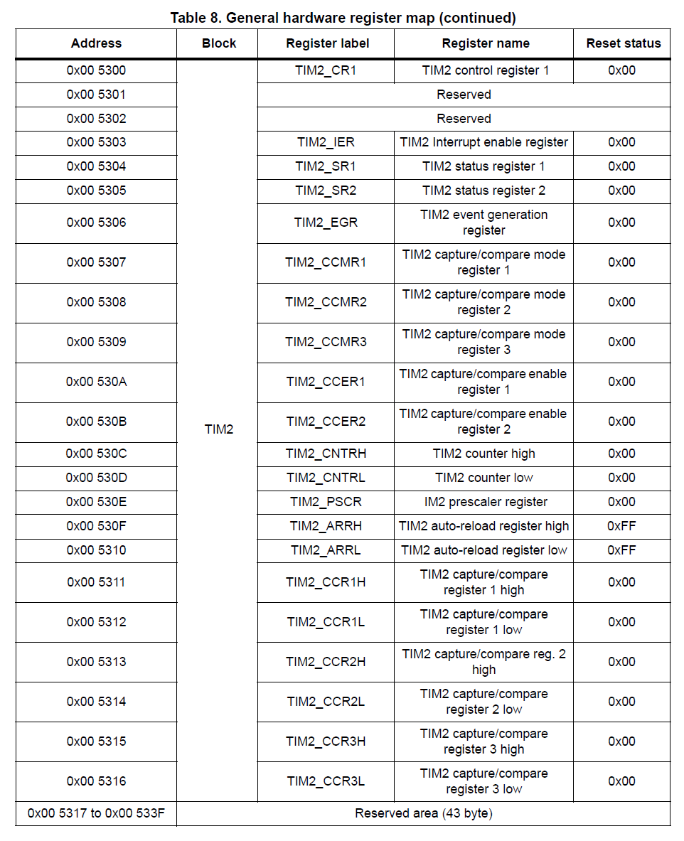
In the next line, we set the prescaler value in the TIM2_PSCR register to divide the common 2 MHz input clock to the timer. The prescaler is a 4-bit value which acts as an exponent to the binary base (2).
MOV TIM2_PSCR, #5 ; Set the prescaler to divide the clock by 32The timer count frequency is determined by,
Timer fc = 2 MHz / 2PSCR
With a prescaler of 5, the TIM2 input frequency becomes,
Timer fc = 2 MHz / 25
         = 2 MHz / 32
         = 62500 = 62.5 KHz
With an auto-reload value of 31250, the effective update frequency becomes,
Timer fu = 2 MHz / 25 / 31250
         = 2 Hz = 0.5 S
So with the current TIM2 configuration, we get around 0.5 second update interrupt rate.
In the next line, we enable the update interrupt (UIE) which is a peripheral interrupt associated with timers.
BSET TIM2_IER, #0 ; Enable update interruptThe update interrupt is triggered whenever the timer is updated with an auto-reload value.
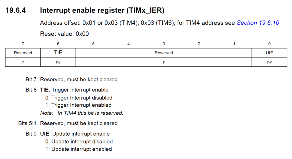
TIMx_IER register descriptionRIM
After configuring the timer, we can enable the global interrupts by unmasking the interrupts with the following line.
RIM ; Enable interruptsThe RIM instruction resets the interrupt enable mask by making I1 flag in CC to 1, and I0 to 0 (lowest priority). The RIM instruction is not needed before a call to WFI and HALT instructions as they do the operation of RIM instruction already.
After enabling the interrupts we can enable the timer with the following line, by making the CEN (Counter Enable) bit in TIM2_CR1 (TIM2 Control Register 1) to 1.
BSET TIM2_CR1, #0 ; Enable the timerWFI
The next instruction is WFI (Wait for Interrupt). This instruction stops the CPU clock and also sets CC.I1 = 1, CC.I0 = 0. Since there is no clock to the CPU, the CPU stops running and it saves power. The CPU will only start working when an internal or external interrupt occurs. In this case, the TIM2 update interrupt will cause the CPU to wake up and run again.
loop:
    WFI           ; wait for an interrupt
JP loop ; loop foreverWhen the WFI instruction is executed, the CPU stops. So the JP is never gets executed. But it is required to complete the logic. The two instructions form a loop indicated with a label loop. Even though we are not doing any useful work here, we can have some task running here instead of the WFI instruction. But for this tutorial we will keep it simple for now.
IRET & BRES
The next is a function we use for running when the TIM2 update interrupt fires. All of the instructions are familiar except the IRET. It is a special return instruction to be used when entering an ISR (Interrupt Service Routine).
; TIM2 update/overflow handler
.func tim2_overflow
    BCPL  PB_ODR, #LED  ; Toggle the LED pin
    BRES  TIM2_SR1, #0  ; Reset timer's update interrupt flag
    IRET
.endfWhen entering the function, we first toggle the LED pin state by changing the bit on the output data latch register. When the timer update interrupt is fired, the UIF (Update Interrupt Flag) of the timer status register TIM2_SR1 is set. So a 1 in that flag means an update is pending. When it is pending, no more interrupts will be generated. So we need to manually clear it so that the next update interrupt can fire. This is done with the help of the BRES instruction. Similar to BSET, but instead of setting a bit to 1, the BRES resets the bit to 0. After that we can call the IRET instruction which restores the contents of PC, A, X, Y and CC from the stack.
Finally, we set the interrupt vectors. The reset interrupt vector is set to the start of the program indicated by the label start.
; Interrupt vectors
.org 0x8000
    INT  start           ; RESET handler, jump to the main program body

.org 0x803c
INT tim2_overflow ; IRQ13: TIM2 update/overflow interruptAs per the datasheet, the IRQ number 13 corresponds to the TIM2 update/overflow interrupt and the location is 0x803C. So all we have to do is to set the address of the tim2_overflow function at that interrupt vector location. Whenever the TIM2 update interrupt is fired, the function tim2_overflow is executed.
The result is the same as our previous blink sketch. But now instead of wasting time of the CPU using NOP instruction, the CPU can do something useful. Though we are not doing anything here at the moment. We will show you in a future tutorial how you can blink the LED in a constant rate, and at the same time respond to push-button inputs. Whenever the push-button is pressed, the LED blink rate will be changed.
Assembling & Uploading
The program can be assembled and uploaded the same way we have done before. Use the following command to assemble.
naken_asm main.asm -o main.hex -type hex -lFollowing is the NakenASM log output after a successful assembling.
PS D:\Code\Naken-ASM\STM8\Blink-Timer> naken_asm main.asm -o main.hex -type hex -l

naken_asm

Authors: Michael Kohn
         Joe Davisson
    Web: https://www.mikekohn.net/
  Email: mike@mikekohn.net
Version:

 Input file: main.asm
Output file: main.hex
  List file: main.lst

Pass 1...
Pass 2...

Program Info:
Include Paths: .
               /usr/local/share/naken_asm/include
               include
 Instructions: 16
   Code Bytes: 51
   Data Bytes: 0
  Low Address: 0x8000 (32768)
High Address: 0x80aa (32938)Below is the generated hex file.
:0480000082008080FA
:04803C00820080A29C
:108080009B721A5007721A5008357A530F351253E3
:10809000103505530E721053039A721053008FCC93
:0B80A000809E901A500572115304805E
:00000001FFTo upload, run the following command.
stm8flash -c stlinkv2 -p stm8s003f3 -w main.hexBelow is the upload log.
PS D:\Code\Naken-ASM\STM8\Blink-Timer> stm8flash -c stlinkv2 -p stm8s003f3 -w main.hex
Determine FLASH area
libusb: error [init_device] device '\\.\USB#VID_1A2C&PID_99FD&MI_01#7&1F2B3ED5&1&0001' is no longer connected!
libusb: warning [force_hcd_device_descriptor] could not infer VID/PID of HCD hub from '\\.\ROOT#USB#0000#{3ABF6F2D-71C4-462A-8A92-1E6861E6AF27}'
libusb: warning [force_hcd_device_descriptor] could not infer VID/PID of HCD hub from '\\.\ROOT#USB#0000#{3ABF6F2D-71C4-462A-8A92-1E6861E6AF27}#UDE'
Due to its file extension (or lack thereof), "main.hex" is considered as INTEL HEX format!
171 bytes at 0x8000... OK
Bytes written: 171The LED will start blinking as soon as the uploading is completed.
What’s Next
In the next tutorial, we will learn how to interface a simple tactile push-button with the microcontroller and control the blink rate of an LED. We will demonstrate both polling method and interrupt method to read the push-button. Check out the next tutorial below.
Reading Push-Buttons Through Polling : Learn Microcontroller with STM8S – Tutorial Part #6
Links
- What is A Microcontroller? : Learn Microcontroller with STM8S – Tutorial Part #1 – CIRCUITSTATE Electronics
- NakenASM – Official Website
- NakenASM – GitHub
- STM8 Assembler Playground
- STM8S Series – Official Product Page
- STM8S103F3 Datasheet [PDF]
- AN2752 – Getting Started with STM8S and STM8AF Microcontrollers [PDF]
- PM0044 – STM8 CPU Programming Manual [PDF]
- RM0016 – STM8S and STM8AF Series 8-Bit Microcontrollers [PDF]
- STM8 Product Lineup [PDF]
Short Link
- A short URL to this page – https://www.circuitstate.com/stm8blinkwithtimer


