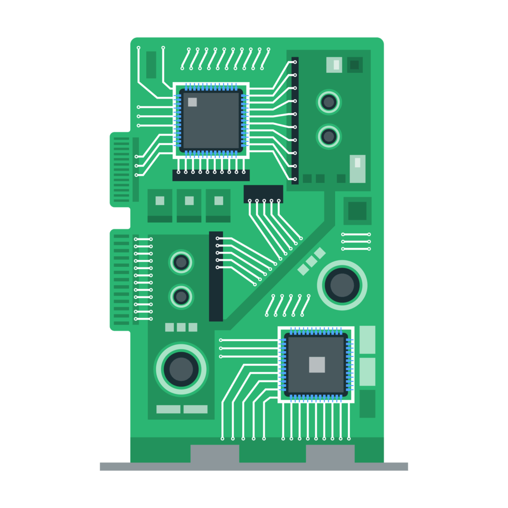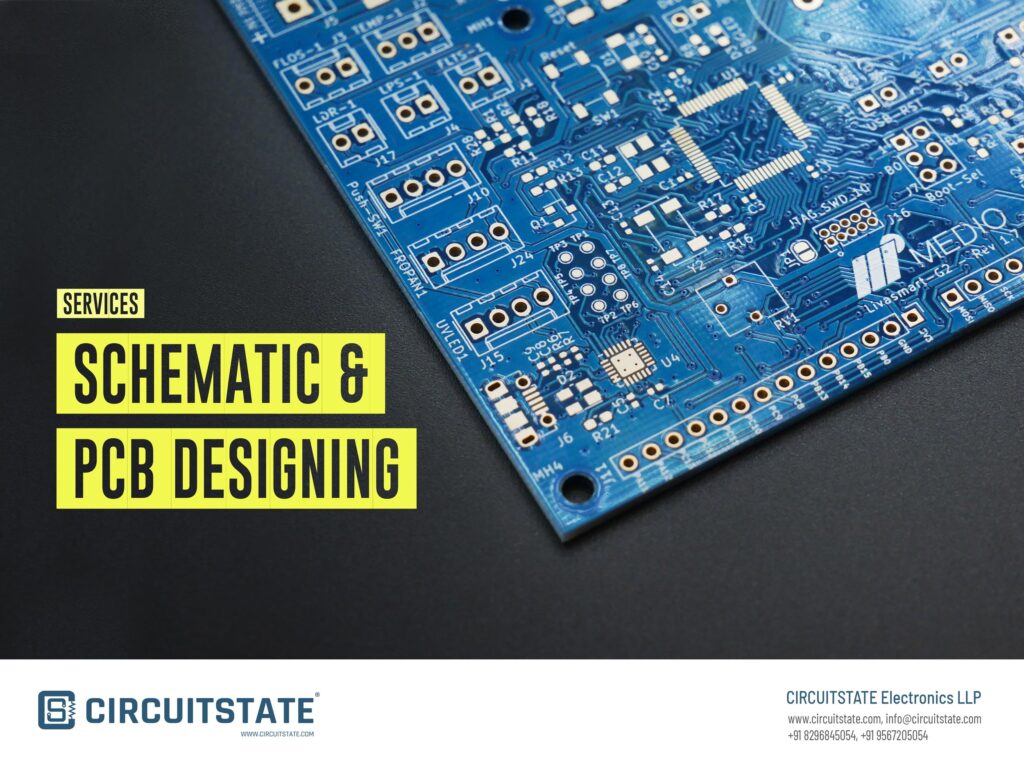
A Printed Circuit Board (PCB) is a rigid or flexible backplane that retains and interconnects all electronic components that are part of an electronic circuit. A PCB is created from a graphical circuit design called a schematic and components are then arranged on a board layout. PCBs are an integral part of any electronic product and optimizing the size and cost of PCBs are important to make the product reliable and affordable.

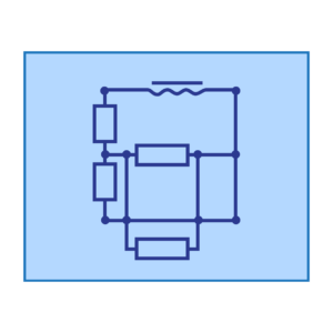
This process takes care of drawing a graphical representation of the circuit, called a schematic. Designing a schematic is called schematic capture. Every electronic/electrical component is given a unique symbol to identify them in the schematic. Each component has its pins numbered and labeled according to part datasheets. These pins are connected to other components via lines of different forms. The schematic will also have a netlist which is the information that conveys what components are connected to where. An annotated and verified schematic file is used to create a PCB layout. The schematic can also be printed on paper for reference. Tools like KiCad, Altium Design, OrCAD, and DipTrace can be used to draw schematics.

Once the schematic is complete, the netlist can be used to create a physical PCB design layout. Each component on the schematic has its physical layout called a footprint. The components are inserted/placed on these footprints and soldered on a board. PCB design takes care of placing these footprints on a desired layout and connecting them using tracks and vias. The board layout or shape can be anything according to the mechanical design of the electronic product. A PCB can have one or more conductor layers. Once the design is finished, files suited for manufacturing can be exported and sent for fabrication. The files required for fabricating PCBs are called Gerber files. Tools like KiCad, Altium Design, OrCAD, and DipTrace can be used to draw PCB layouts.
Gerber files, along with other files are sent to a fabrication house for production. The fab house will check and verify the design (DFM check) to determine if it conforms with their manufacturing capabilities. Sometimes you have to communicate with the fab house to sort out any design issues. We usually take care of this process. Once the files are approved, the fab house will give us estimates on production time and cost. The fabricated PCBs undergo many types of quality inspection stages such as optical testing, X-ray testing, flying probe testing, etc. We can work with all types of manufacturers from all regions to get you the least turnaround time.
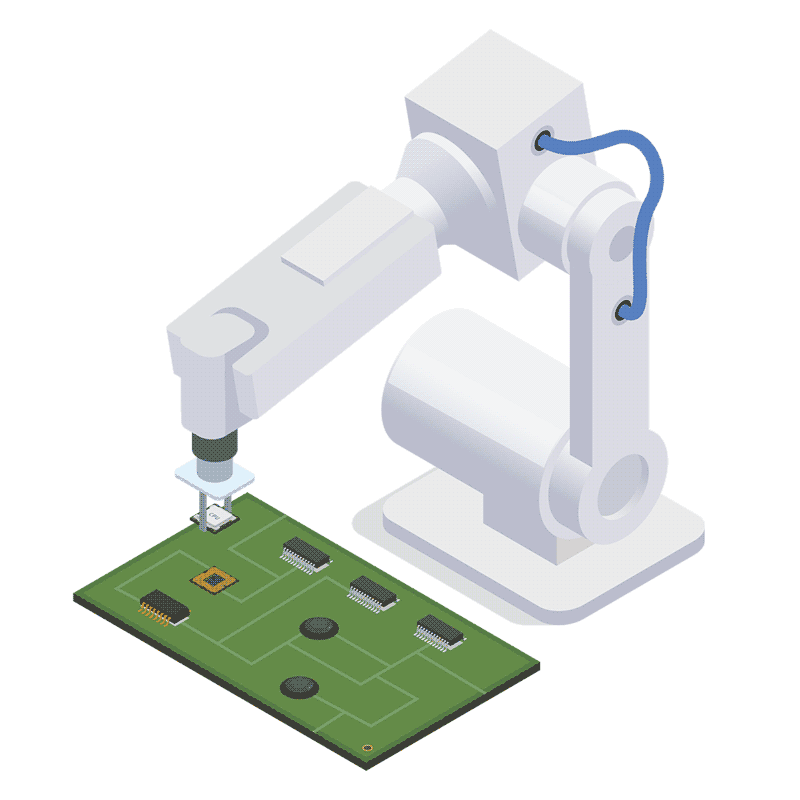
PCBs have to be assembled with their components to fully test them. This can be done manually or automated. Automated PCB Assembly (PCBA) uses computer-controlled machines to place components on multiple PCBs at a time and solder them together. This saves time and cost of production as the machines can do the assembly processes much faster than humans. A different set of files are required for automated PCB assembly. We also take care of generating fabrication files and sending them to the assembly house. We can also help you optimize your product BoM (Bill of Materials) by choosing components with the lowest price and long production life.
Tell us about your requirement
Get the most cost-optimized and efficient PCB design from us, with quality documentation and support through various stages.
