PBSEQ-D2 – Soft-Latching Power Sequencer Circuit using MOSFETs & Push-Button
Learn how to use basic electronic components like Mosfets and Push-Buttons to make a soft-latching power sequencer circuit to control power to your projects.
Switches are a simple yet very important piece of technology that is still used almost everywhere. To have a switch is to have control of something. Modern technology has advanced so much that you don’t even need a switch at all. You could turn on your device by just asking it because such devices are always on, and consume very little power to remain so. Still, we use switches; because they are simple and cheap. Even the latest Raspberry Pi 5 has a new switch. You can turn on your RPi 5 with a single push of a button. That is not the kind of switch that we are familiar with though. Most of the switches for power control are a type of flip-switch with some mechanical latching mechanism. It is a bistable device that can remain in either of the two states indefinitely. But what if you wanted a switch that is not mechanical but still able to control power whenever you press it, instead of flipping? You could obviously use a microcontroller or some other active devices for that. But wouldn’t that be an overkill? What if we told you that you could create a soft-latching power switching circuit (power sequencer) with a few discrete components? Read on.
Circuit Diagram
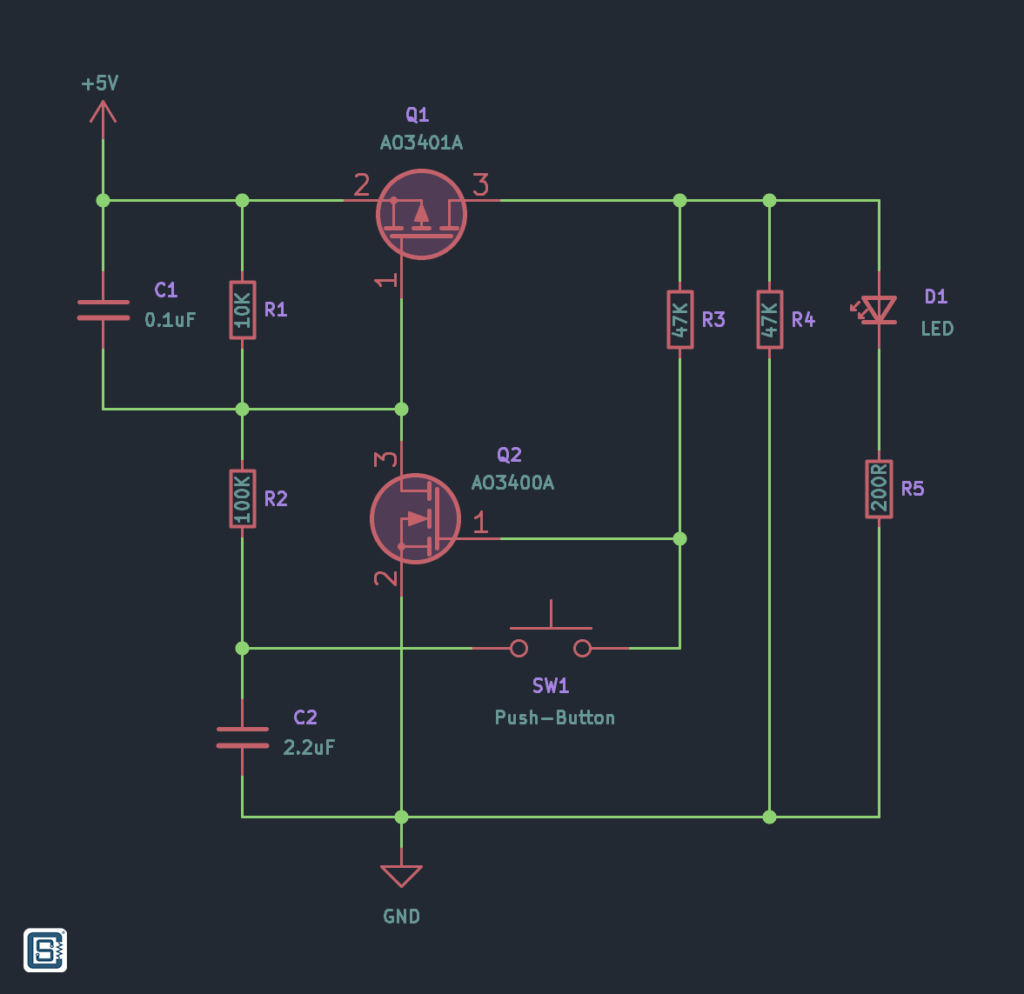
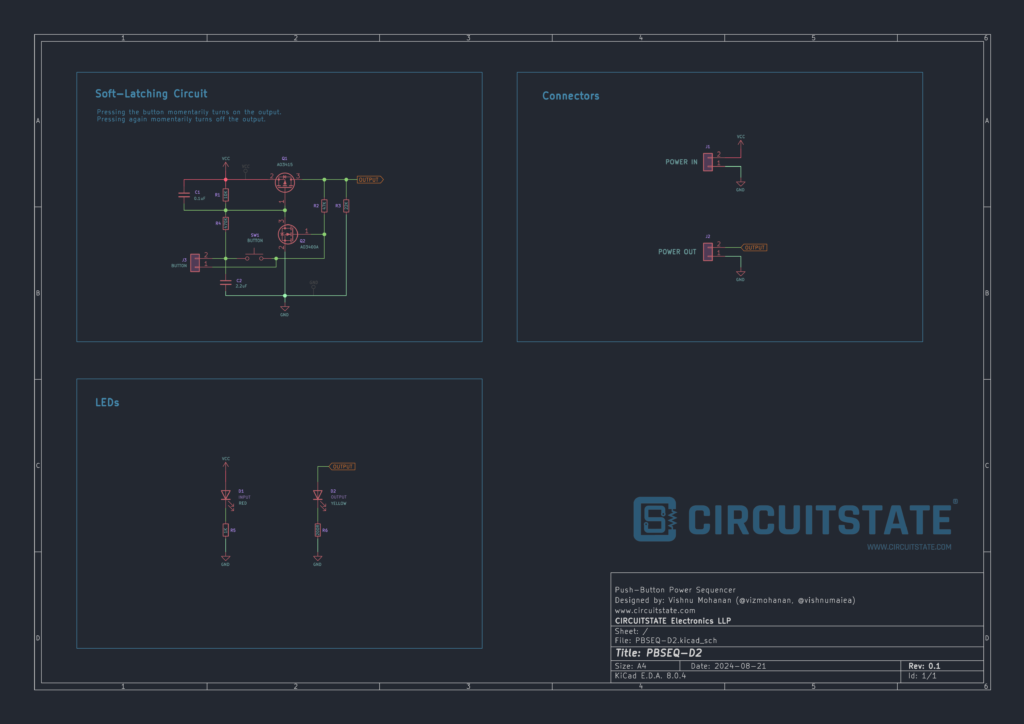
The circuit consists of 8 discrete components if you discount the LED and its resistor. Q1 is a P-Mosfet and Q2 is an N-Mosfet. We are using the AO3400A and the AO3401A complementary pair of Enhancement-Mode Mosfets here. But you could use almost any small-signal Mosfets here. Q1 acts as a high-side load switch. When the voltage on its gate pin is more positive, the transistor turns off and when the voltage is relatively more negative, the transistor turns on. For the N-channel Q2, the behaviour is the opposite; you need a positive voltage to turn it on and a negative voltage to turn it off. Q2 is used as a low-side switch, which means, it connects the gate of Q1 to the GND when it is on.
R1, R2, and C2 form a simple RC network. The R1 and R2 also form a voltage divider whose output is connected to the gate of Q1. The duty of C1 is to apply a positive pulse to the gate of Q1 when the circuit is initially powered on in order to keep the transistor off. R3 is a feedback resistor and R4 is a small load to make sure there is always a discharge path on the output.
When the circuit is first powered on, Q1 remains in the off state, thanks to C1, which injects a positive pulse to the gate of Q1. C2 also starts to charge to the supply voltage through combined R1 and R2 resistances which is 110K in this case. The time it takes for the capacitor to fully charge can be calculated with the RC time constant equation.
Time (S) = R (Ohms) x C (Farads)
C2 will charge quickly enough. Once it is charged, the voltage at the gate of Q1 remains at a positive level, thus keeping the Q1 off. At the same time, Q2 also remains off. This is because it needs a positive voltage on its gate but since Q1 is off, there is no way it can get that positive signal. This is the first state of our circuit; the on state.
But things take a turn when you press the SW1 push-button. When you momentarily press it, the positive potential saved in the C2 capacitor suddenly will appear on the gate of Q2, and turning it on. If Q2 is turned on, that means it will pull the gate of Q1 to the ground thereby turning it on in a chain reaction of events. C2 will also discharge through Q2 since it is now a low-resistance path to the ground. With the Q1 turned on, we now get power through the drain pin of the P-Mosfet which will turn on the output LED.
So with a single press of the push-button, we changed the state of the circuit from the off state to the on state. This is the second state of the circuit and it can remain in either of the two states indefinitely until we actuate the push-button. So what happens when we press the button again when the circuit is on? Go on try it.
Remember that, when the circuit output is on, the C2 capacitor remains in a discharged state. When you press the button, C2 will start to charge through R3 initially. This will drop the voltage on the gate of Q2, thus turning it off. But the path of the current to C2 immediately changes to R1 and R2 since Q2 is now in the off state. You know what happens when C2 is charged? Yes, Q1 is turned off, and with Q2 now in the off state, Q1 has no way to turn on again until we do something about it. So we just switched to the off state of the circuit and achieved the toggling action with the press of a single push-button. You can press the button again and again to see the toggling in action.
Simulation
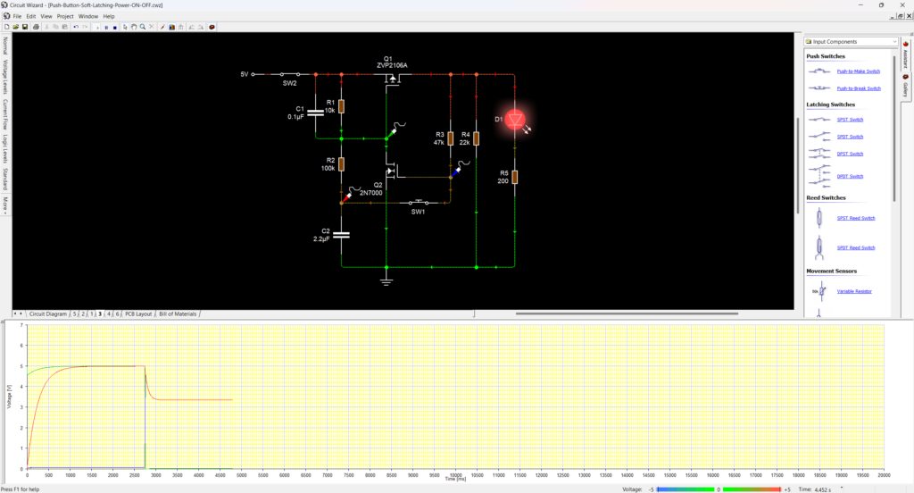
Was the previous working explanation too confusing? Well, explaining circuits becomes better with a simulation. We will use Circuit Wizard, a SPICE-based circuit simulator for this. In the below circuit, we have three voltage probes to monitor the voltages on those points.

The following screenshot shows the initial state of the circuit when powered on for the first time. You can see that the capacitor C2 is being charged via R1 and R2. The arrows indicate the direction of current flow at that instant. In the graph, the green line is the voltage on the gate of Q1 and is seen increasing to a positive potential which keeps it turned off.
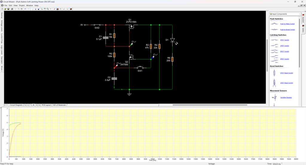
When the push-button SW1 is pressed, however, the voltage on the C1 appears on the gate of Q2, causing it to turn on momentarily. This starts to discharge the C2 through Q2 as you can see from the direction of currents. Since there is a positive potential at the gate of Q2, it is turned on and thus keeps the Q1 turned on. You can also see on the graph how the C2 is discharged.

When the button is pressed again, this time when the output is on, C1 starts to charge up again, causing a low voltage at the gate of Q1. Once C1 is fully charged, it keeps the gate of Q1 low and therefore keeps it off. The effect is carried to the gate of Q2 as a low potential and therefore turns it off. The circuit is now in its off state and will remain in that state indefinitely until the button is pressed again.
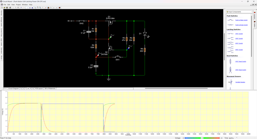
If you press the button again and again, the state of the circuit will toggle alternatively.

So every time you press the button, the state is toggled. This gives us the behaviour we need for a single push-button-controlled power switching circuit. But what happens when we keep the button pressed?
If the circuit was in the on state and you press and hold the button, the circuit will turn off instantly when you press it and remain off. The voltage on the gate of Q1 will be close to 5V and the voltage of the C1 capacitor will be at around 2V because it can’t charge further due to the discharging effect through the load resistance.

On the other hand, if the circuit was in the off state and you press and hold the button, the circuit will turn on instantly and remain on. This is because pressing the button momentarily is enough to turn on the circuit. Since Q2 is already pulling the gate of Q1 to ground, the capacitor C1 is not charged beyond 4V, and therefore has no effect on the state of Q1.
Following is the video of the simulation.
PCB Design
Circuit design based on an idea and simulating it got us so far. But that is not enough. Designing an electronic circuit is equivalent to programming. Instead of using the usual programming constructs such as if, else, while, etc., we have to use electronic components as our logical components. Each component has a specific behaviour depending on where it is used. We take advantage of those behaviours to implement a circuit. But in order to be sure that the circuit will work, we need to physically make it and test it. This is like running a program and debugging it. We need to check if the circuit works correctly, and find out why if it doesn’t.
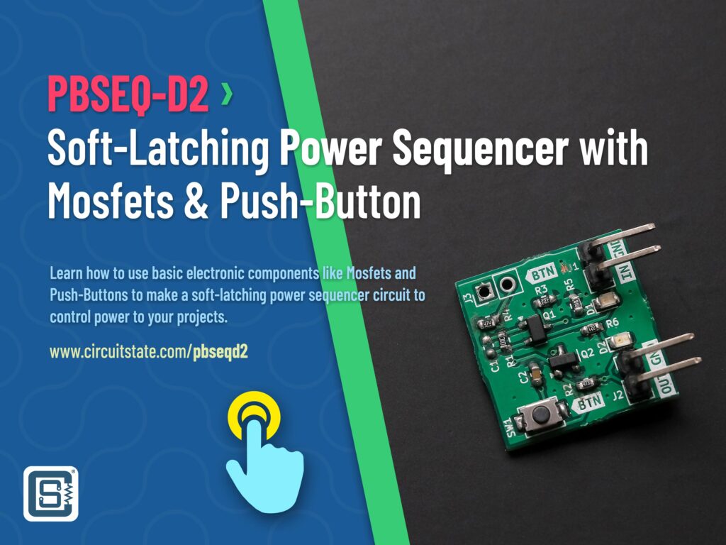
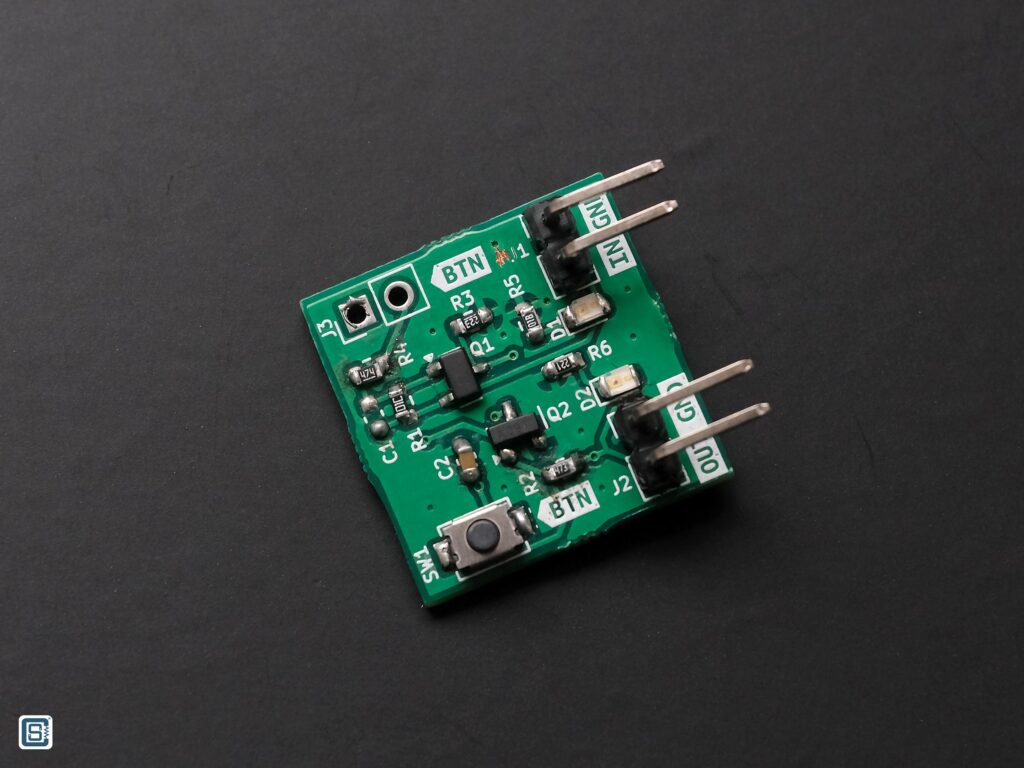
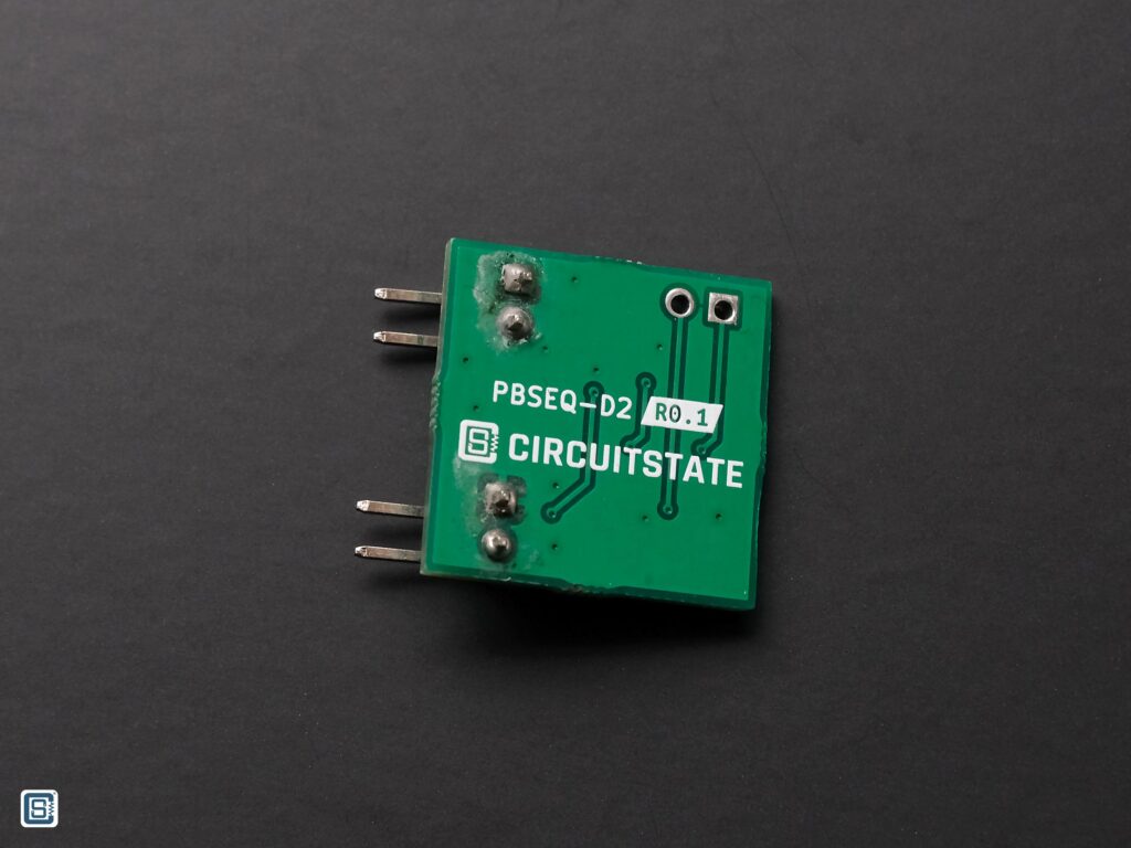
We designed a small PCB using KiCad to test this circuit, called PBSEQ-D2. The PCB has 19 x 19 mm dimensions. It is not the smallest we can make this circuit. But for the sake of testing and handling, we should limit how small the design going to be. We fabricated the PCBs from Lion Circuits. The PCB design source files are open and you can download them from our GitHub.
Following is the schematic. We are using 10K and 470K resistor values here for the initial voltage divider.
Following are screenshots of the PCB design.
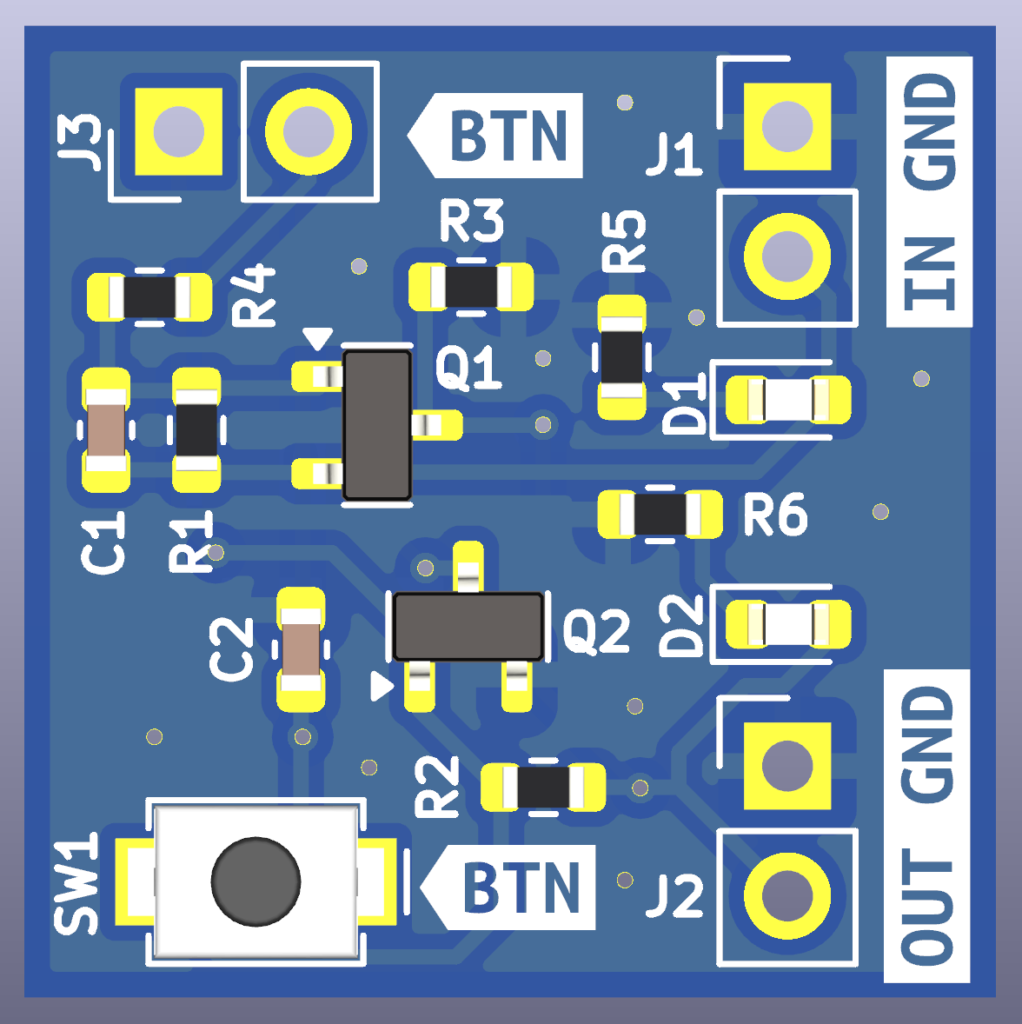
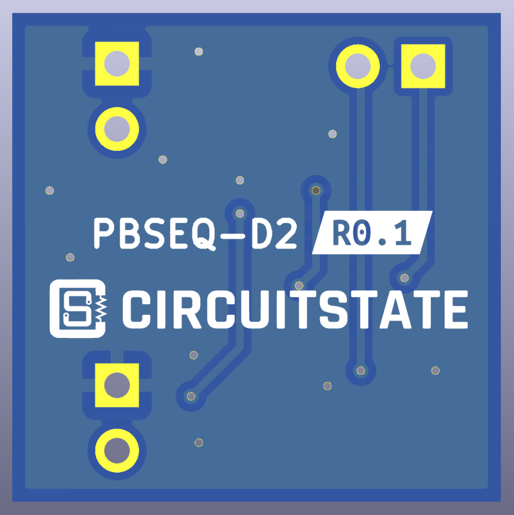
In this configuration, with a supply voltage of 5V, we get around 2 seconds delay between ON and OFF states. That means, we can only turn off the output after two seconds of turning it on. That is a useful advantage that will prevent unintentional turning offs and reduce the effect of push-button bouncing. The delay remains the same even if we reduce the voltage to 3V. At 8V, the time is around 3.5 seconds. At 10V, the delay is around 6 seconds. The time delay increases because the charge collected by the capacitor increases and it takes a longer time for it to discharge through the fixed value resistors. At 12V, the circuit won’t turn off and instead blink momentarily. The circuit will also turn on if we touch the junction of C2 and R4. I think stray voltages cause the Q1 to go into conductive mode, thus latching the output to ON.


Links
- Latch and Toggle Power Circuits – Mosaic Documentation Web
- RC Charging Circuit – Electronics Tutorials
- PBSEQ-D2 by CIRCUITSTATE – GitHub
- Circuit Wizard – New Wave Concepts
- AO3401A – P-Channel Mosfet – Datasheet [PDF]
- AO3400A – N-Channel Mosfet – Datasheet [PDF]
Short Link
- Short URL to this page – https://www.circuitstate.com/pbseqd2


