STM8S-Blue Generic STM8S103F3P6 Development Board – Pinout Diagram & Pin Reference
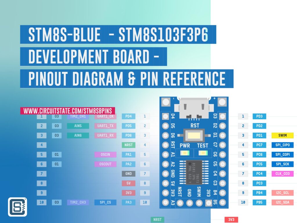
Vector pinout diagram and pin reference for the STM8S103F3P6-based STM8S-Blue 8-bit microcontroller development board.

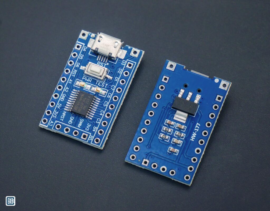
STM8S-Blue is a generic STM8S103F3P6 microcontroller development board available in the market. It is a minimum system development board that integrates a USB connector, a 3.3V voltage regulator, a reset button, and two LEDs in addition to the 20-pin microcontroller. STM8S103F3P6 is a low-cost 8-bit microcontroller from ST Microelectronics. On this page, you will find a vector pinout diagram for the STM8S-Blue board. The name of the board is not official, but a generic one. People call it the blue board since the color of the PCB is blue.
Features

| Specification | Value |
|---|---|
| CPU | STM8S103F3P6 |
| Series | STM8S |
| Clock | 16 MHz (Internal) |
| Flash | 8 kB |
| RAM | 1 kB |
| EEPROM | 640 bytes |
| I/O voltage | 3.3V |
| GPIO | 14 |
| Interface ports | UART, SPI, I2C |
| PWM | 4 (up to 7 via alternate mapping) |
| ADC | 5-channel, 10-bit |
| LED | PB5 (Arduino D3), active low, shared with I2C, red |
| Program/Debug Interface | SWIM |
| USB | Micro-USB (power only) |
| Dimensions | 18 x 30 mm |
Schematic
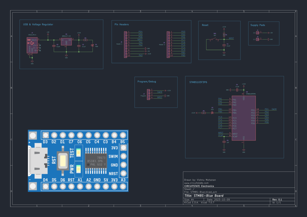
We could not find an accurate schematic diagram of the STM8S-Blue board on the internet. We created one ourselves using KiCad. The schematic is based on the exact STM8S-Blue we have. You can download the schematic as an image, PDF, or the KiCad source file.

Pinout Diagram
Latest Revision: Rev 0.1, 09-10-2023
Design by: Vishnu Mohanan
License: CC-BY-SA 4.0
There are no official references for the pinout of STMS-Blue. Since these boards come mainly from no-name manufacturers in China, there is no guarantee of pinout compatibility or product quality. We used the boards we already have as the reference for creating these pinouts. While we try our best to be accurate and up-to-date here, we can not guarantee correctness. We have seen boards with conflicting pinouts and pin labels. So please also double-check the pin assignments with that from the official documentation. If you find any errors, please let us know in the comments.
PNG

PDF preview may not load on mobile devices. Click the link to open an interactive preview, or download it directly.
Pin Reference

| Pin # | GPIO | High Sink | Speed | Main Alt. Function | Alt. Function |
|---|---|---|---|---|---|
| 1 | PD4 | HS | O3 | BEEP/TIM2_CH1/UART1_CK | – |
| 2 | PD5 | HS | O3 | AIN5/UART1_TX | – |
| 3 | PD6 | HS | O3 | AIN6/UART1_RX | – |
| 5 | PA1 | – | O1 | OSCIN | – |
| 6 | PA2 | – | O1 | OSCOUT | – |
| 10 | PA3 | HS | O3 | TIM2_CH3 | SPI_CS (AFR1) |
| 11 | PB5 | X | O1 | 12C_SDA | TIM1_ BKIN (AFR4) |
| 12 | PB4 | X | O1 | 12C_SCL | ADC_ETR (AFR4) |
| 13 | PC3 | HS | O3 | TIM1_CH3 | TLI (AFR3), TIM1_ CH1N (AFR7) |
| 14 | PC4 | HS | O3 | CLK_CCO/TIM1_CH4/AIN2 | TIM1_CH2N (AFR7) |
| 15 | PC5 | HS | O3 | SPI_SCK | TIM2_CH1 (AFR0) |
| 16 | PC6 | HS | O3 | SPI_COPI | TIM1_CH1 (AFR0) |
| 17 | PC7 | HS | O3 | SPI_CIPO | TIM1_CH2 (AFR0) |
| 18 | PD1 | HS | O4 | SWIM | – |
| 19 | PD2 | HS | O3 | AIN3 | TIM2_CH3 (AFR1) |
| 20 | PD3 | HS | O3 | AIN4/TIM2_CH2/ADC_ETR | – |
- Only GPIO pins are shown.
- Default function of all GPIO pins after reset is port GPIO.
- – – Not applicable
- X – Not available
- Ox – Speed Class
- O1 – Slow (up to 2 MHz)
- O2 – Fast (up to 10 MHz)
- O3 – Fast/slow programmability with slow as default state after reset
- O4 – Fast/slow programmability with fast as default state after reset
Links
Short Link
- Short URL to this page – https://www.circuitstate.com/stm8sbpins


